the Creative Commons Attribution 4.0 License.
the Creative Commons Attribution 4.0 License.
 | 27 Feb 2020
Morphological characterization and porosity profiles of tantalum glancing-angle-deposited thin films
Tobias Ott
Gerald Gerlach
Glancing angle deposition (GLAD) is a physical vapor deposition (PVD) process using a substrate that rotates tilted at an angle to the evaporation source. Depending on the deposition conditions, it provides the controlled formation of regular nanostructures during the PVD process. As a result, a wide variety of shapes, such as spirals or vertical columns, can be easily fabricated in the nanometer range. For this reason, GLAD has already been proven reliable in the production of optical coatings with very low reflectance in a broad spectral range.
This paper examines the morphology of tantalum nanostructures deposited on planar silicon substrates by electron beam evaporation. The prepared samples are characterized by scanning electron microscope (SEM) images at a breaking edge with respect to the layer structure and by focused ion beam (FIB) SEM images of the cross-sectional areas with respect to the porosity. The porosity can be used to model the optical properties of the thin film with the effective medium theory (EMT). Our work studies the relationship between the evaporation parameters (growth pitch and deposition angle) and thin film morphology of tantalum so that in future work the optical properties can be linked to the deposition parameters, which in turn can be chosen to achieve highly absorbent infrared radiation layers, e.g., for infrared sensors. It was shown that the porosity across the film thickness of both columnar and screw-like thin films is nearly constant, whereas the porosity profiles of spiral structures show a periodic pattern, the period of which seems to depend on the growth pitch.


Thermal infrared (IR) sensors are used for many purposes in noncontact temperature measurement, motion control, gas analysis, fire detection, thermal imaging and many other fields like process control, safety and security as well as the health industry (Budzier and Gerlach, 2011). They absorb the incident IR radiation and transform it into a corresponding temperature increase in the sensor element, which in turn is measured by means of temperature-sensitive transducers, e.g., pyroelectric elements, thermopiles or bolometers.
The thermal resolution of a pyroelectric sensor is directly proportional to the absorption of the sensor element (Budzier and Gerlach, 2011) so that it should be as high as possible. Absorption layers should be as thin as possible to keep their heat capacity low, which is required for fast and high-responsive thermal IR sensors (Schossig, 2012b; Blevin and Geist, 1974).
GLAD is a special deposition process for thin films, which belongs to the PVD (physical vapor deposition) processes. It features deposition under grazing incidence with very high deposition angles α of more than 80∘ and substrate rotation (Robbie, 1998). By rotating and tilting the substrate around the deposition angle, porous thin films can be deposited whose structure can be influenced in the nanometer range (Robbie et al., 1995; Robbie, 1998).
In this paper we investigate the influence of the deposition angle, deposition rate and continuous substrate rotation speed on the morphology of thin films, in particular tantalum films. Tantalum is used because it has a volume-specific heat capacity that is 1.5 times lower than that of the often-used nichrome (NiCr). The study focuses on the shape of the deposited tantalum structures, which depends on the ratio of the deposition rate and substrate rotation speed; this is known as growth pitch. Another important parameter of our study is the porosity across the layer thickness, which strongly depends on both the deposition angle and the growth pitch.
The use of GLAD is not limited to optical applications, like absorption layers for infrared detectors (Schossig et al., 2010) or solar cells (Gonzalez-Garcia et al., 2011). It has been applied in photonic crystals (Kennedy et al., 2002, 2003), gas sensors (Hwang et al., 2013; Beckers et al., 2013), field emitters (Singh et al., 2004), nanomechanical actuators (Dice et al., 2007) and magnetic devices (Albrecht et al., 2010; Alouach et al., 2005), to name a few.
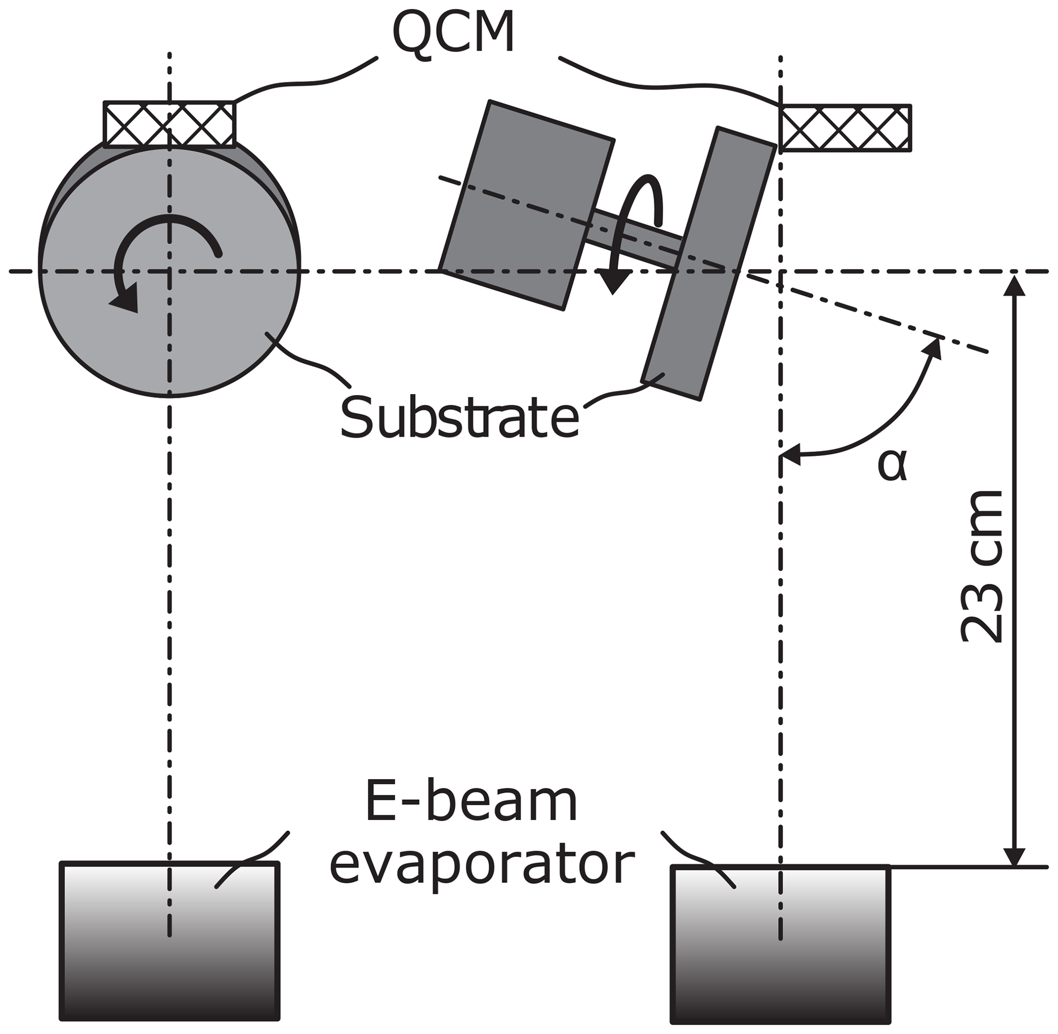
Figure 1 schematically shows the setup of the deposition system used for our GLAD experiments. The tantalum target is heated with an electron beam evaporator and transferred into the gas phase. The distance between the target and the substrate amounts to 23 cm. The substrate is tilted with the deposition angle α and rotating. In this study deposition angles α of 80, 83, 85 and 87∘ were examined. The deposition rate was monitored and kept constant during the entire deposition process using the quartz crystal monitor (QCM) placed in a fixed position in the vacuum chamber and measuring the nominal thickness of the thin films. All films have been deposited with a targeted nominal thickness of 1500 nm. This ensures that the mass flux of the target material is kept constant across all samples. With increasing incidence angle, the real thickness of the deposited thin films is not constant and ranges from 1412 nm at 80∘ to 1116 nm at 87∘ as a result of two opposing mechanisms. The first mechanism causes a decreasing layer thickness with a growing deposition angle due to the decreased projected area of the substrate, which, as a consequence, can accumulate fewer particles. On the other hand, with an increasing incidence angle, the porosity and thus the film thickness increase because the shadowing mechanism intensifies the extinction of adjacent columns. The decreasing film thickness of the investigated samples shows that the latter mechanism does not compensate for the first one.
The growth pitch Pω is used to predict and adjust the shape of the deposited nanostructures:
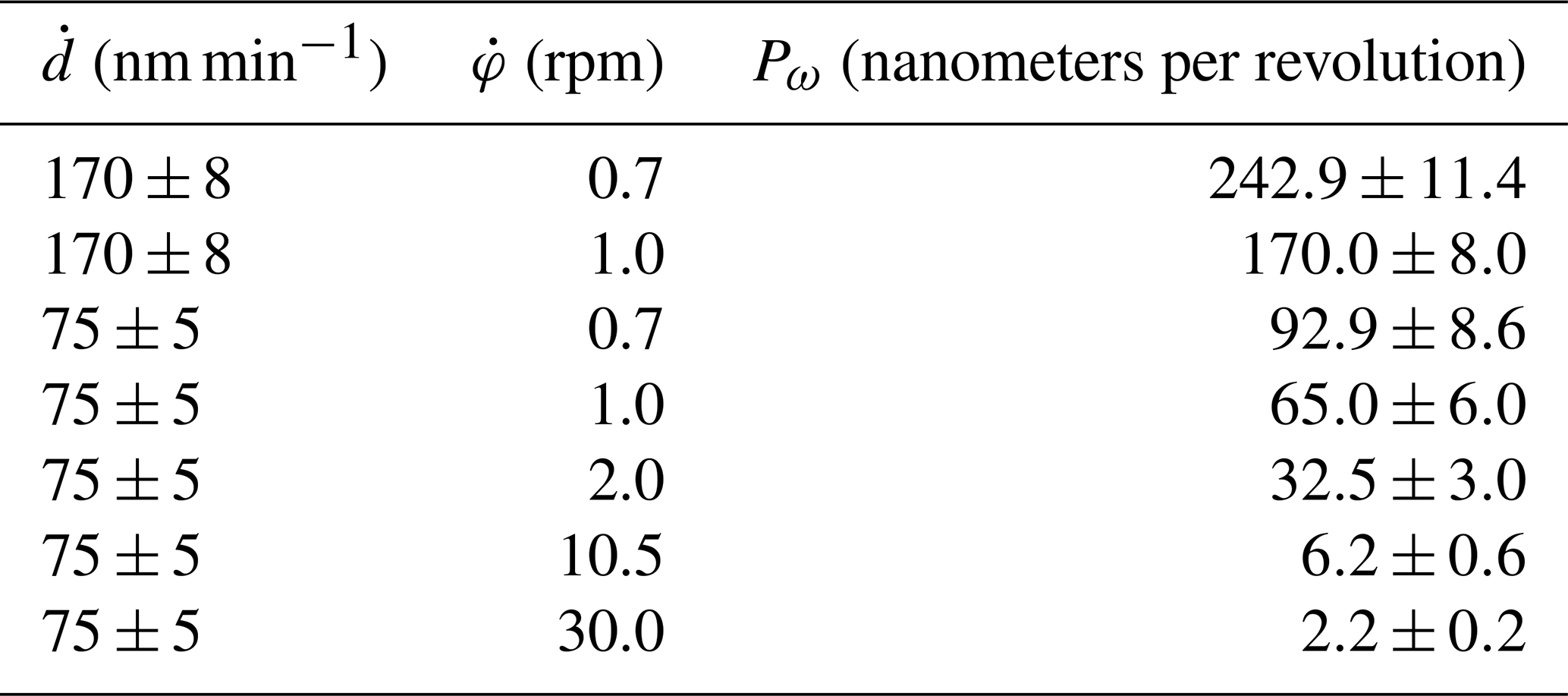
with the deposition rate and the substrate rotation speed . A low growth pitch results in the formation of a columnar film structure (Hawkeye et al., 2014). By increasing the growth pitch, e.g., by reducing the rotation speed of the substrate, the shape of the nanostructures transforms into screws and eventually into spirals. Table 1 summarizes the conditions used for the deposition of the tantalum samples. The wide range of growth pitches enables the deposition of spirals, screws and columns.
Table 1The deposition rate used, substrate rotation speed and resulting growth pitch Pω for the deposition of the tantalum samples.
A substrate temperature above 30 % of the melting temperature of the target material increases the surface mobility of the impinging particles. In this case the substrate temperature can be regarded as a further degree of freedom to influence the layer structure (Hawkeye et al., 2014). To reduce this influence and for better reproducibility, the substrate is cooled actively so its temperature is held below 30 ∘C during the evaporation. As a result, the diffusion length of the adsorbed particles on the substrate surface is reduced to a negligible level. The depositions were performed at a working pressure of (5 … Pa.
The shape and distribution of the nanostructures influence the optical properties of the thin film and depend strongly on the deposition angle and the growth pitch (Hawkeye and Brett, 2007). The optical properties of the nanostructured thin film can be modeled with the effective medium theory (EMT), which aims to replace the heterogeneous, structured thin film with a homogeneous, uniform approximation of it that is more accessible for optical calculations (Landauer, 1978). In the EMT, the effective refractive index neff of the structured thin film is a weighted average of the wavelength-dependent refractive indices n1 and n2 of the two mixed components and the filling factor ρ; the layer structure decides which EMT can be applied, e.g., Garnett (1904, 1906) or Bruggeman (1935).
The sensor operates in an air atmosphere. In this case the filling factor ρ is called porosity. It expresses the mixing ratio of air and tantalum and is defined as
where VAir is the volume of air and VTa is the volume of the tantalum nanostructures in the thin film. Since the refractive indices of the two materials air and tantalum are invariable, the effective refractive index can be influenced by the porosity ρ, which depends strongly on the deposition angle and the growth pitch. By varying these parameters the optical and physical properties can be adjusted as desired.
In order to model the optical properties of the deposited absorption layers, it is necessary to investigate the layer structure in detail in a first step. For this purpose, the porosity distribution of the thin films has to be analyzed based on the given morphology.
3.1 Shape of nanostructures
To describe the morphology of the nanostructures formed after GLAD, their shape has to be analyzed. For this purpose, SEM images were taken from a broken edge of the silicon substrates with the deposited film. In this way, the structure (spirals, screws or columns) can be identified and the layer thickness can be measured.
Figure 2 shows a series of thin layers of tantalum deposited at a deposition angle of α=80∘ but differing in growth pitch Pω. Starting from a low rotational speed and a high deposition rate, which corresponds to a high growth pitch, the deposition rate and rotational speed have been adjusted according to Table 1 in order to achieve a decreasing growth pitch.
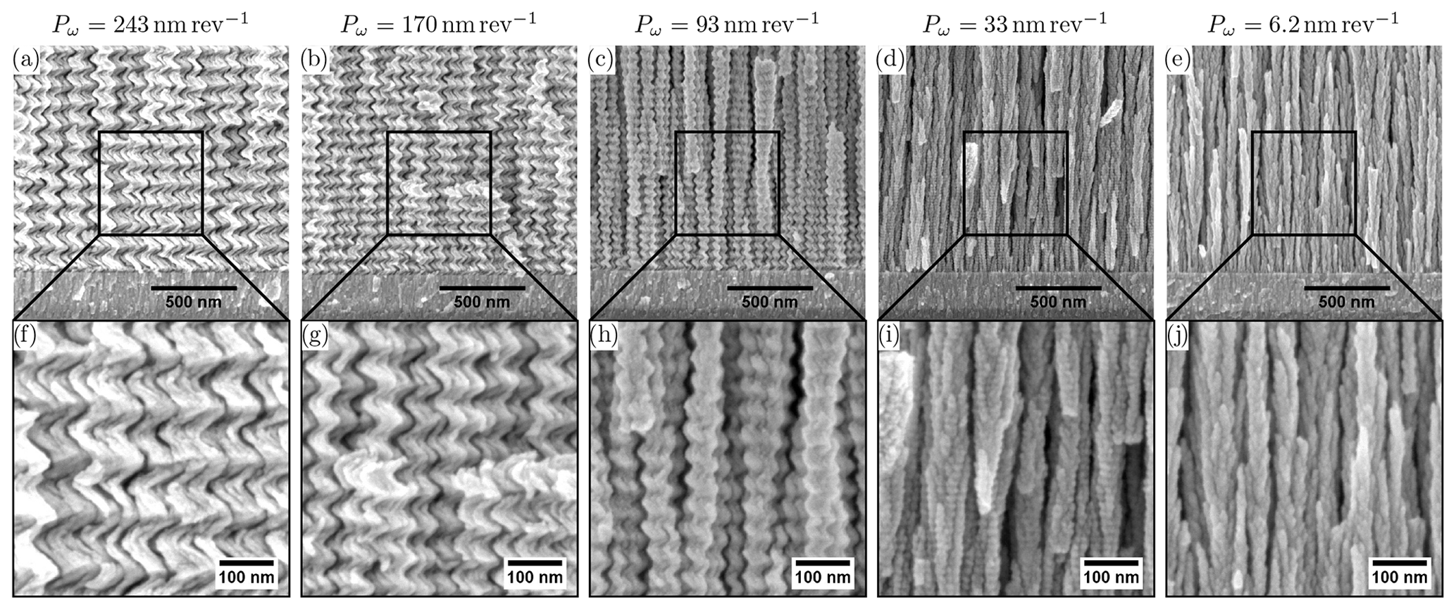
Figure 2(a)–(e) Layer structure and (f)–(j) their magnified view of a series of tantalum structures deposited at a deposition angle α of 80∘ with decreasing growth pitch Pω. The growth pitch can be used directly to adjust the microstructure.
With decreasing growth pitch a significant transformation of the microstructure takes place, whereby different ranges can be identified (Table 2).
Table 2Ranges of the growth pitch Pω and the obtained shape of the deposited structures.
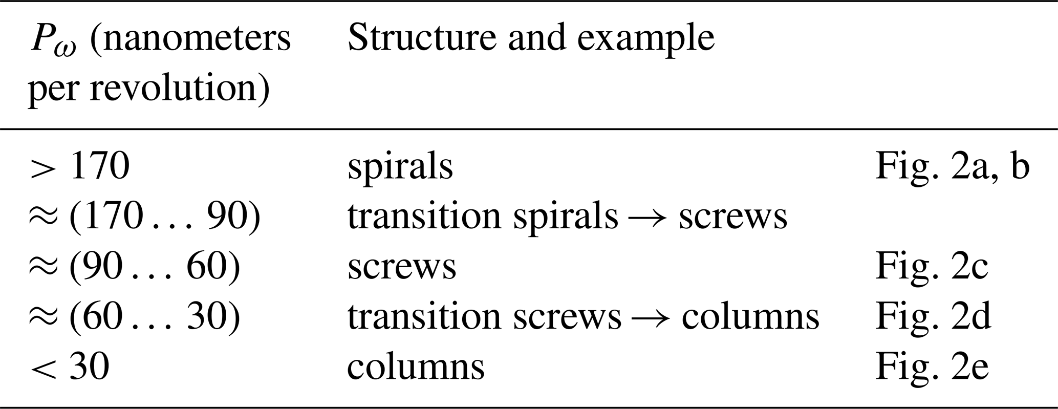
According to Table 1, the deposition rate in Fig. 2a and b is high, whereas the rotational speed is low. This results in a high growth pitch, which produces spirals. With decreasing growth pitch, the spiral cross section is reduced (b) until growth pitch approaches the column width w, thus producing screws (c). If the speed of rotation is further increased, screw-like columns (d) and eventually columns form (e).
3.2 Dominant intercolumn spacing
With the Fourier analysis periodic signals can be examined for their frequency spectrum. Therefore, it is useful to analyze the recurring spatial pattern of GLAD thin films.
A top-view SEM image of a GLAD layer serves as input for the Fourier analysis. The gray values of the individual pixels can be interpreted as a location-discrete, equidistant signal, which is transformed into a discrete frequency spectrum by the discrete Fourier transform. For an efficient calculation, the fast Fourier transform (FFT) is used as an algorithm, which is given for a SEM image with nx pixels in the x direction and ny pixels in the y direction by
where I(x, y) is the grayscale intensity of the image at the (x, y) position, and xf and yf are the spatial frequency coordinates in the x and y directions. To quantify the dominant spatial frequencies, the power spectral density (PSD) (Zhao et al., 2001) is then obtained from the transformed image with the relation
An efficient calculation of the dominant spatial frequencies is achieved when the dimensions of the SEM images in pixels are a power of 2. Therefore, image sections with the pixel dimensions 2048×2048 have been used. The evaluation of the SEM images is done with the free program Fiji (version 1.52e) (Schindelin et al., 2012) and the plugin Parallel FFTJ (version 1.4), which implements the calculations from Eqs. (3) and (4).
Figure 3 illustrates an example for the application of the Fourier analysis on the quantitative analysis of the periodic structure of a GLAD thin film. Fig. 3a shows the top view of an SEM image of a tantalum layer deposited at α=80∘ with a growth pitch Pω of 6.2 nm per revolution. The resulting two-dimensional PSD, as shown in Fig. 3b, has a diffuse ring-shaped structure, indicating the presence of a dominant spatial frequency and thus a dominant distance between adjacent columns. This spatial frequency lies at the ring radius where the PSD is maximum.
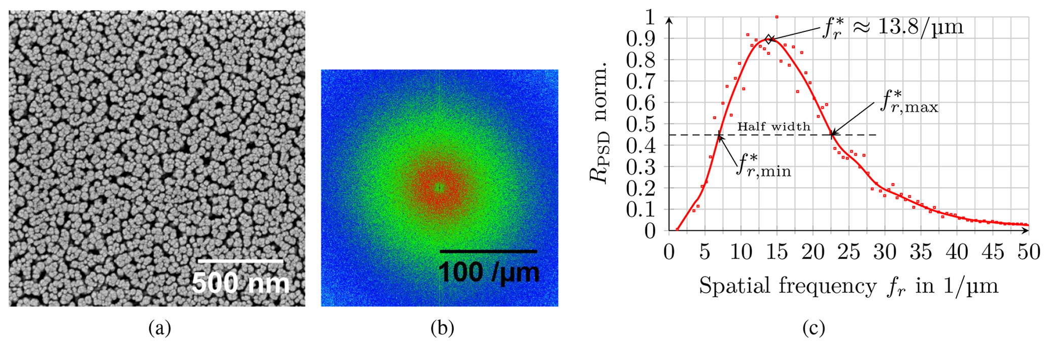
Figure 3Procedure to evaluate the dominant spatial frequency from an SEM image. (a) The starting point is an SEM image of the top view of tantalum columns produced with GLAD; (b) power spectral density of the top view according to Eq. (4), where high gray values are colored red and the ring-shaped pattern is revealed; (c) plot of the angular-averaged power spectral density according to Eq. (5) with marking of the dominant spatial frequency . The range of variation of the dominant spatial frequency is defined by the half-width (dashed line) (Buzea et al., 2005).
The rotational symmetry of the annular structure, derived from an image with the same number of pixels in the x and y direction, shows that vertical columns deposited by glancing angle deposition and fast substrate rotation have an isotropic distribution. In particular for such distributions, it is recommended to calculate the angular-averaged power spectral density RPSD1 (Zhao et al., 2001) by
with the number of pixels nr on the circumference of the circle with the radius fr given by
All points on the circumference of this circle, whose center lies in the center of the PSD image and thus also in the center of the ring-shaped structure, represent a constant spatial frequency fr. The angle between a point on the circumference and the center of the circle represents a direction in the original image. Equation (5) thus averages the power spectral density across all directions in the original image so that the dominant spatial frequency can be read from the maximum of the direction-averaged power density as a function of the spatial frequency (Fig. 3c). Thus, the dominant column spacing r* is
In Fig. 3c the spacial frequency amounts to 13.8 µm−1, and thus the dominant column spacing r* between the structures is approximately 72 nm.
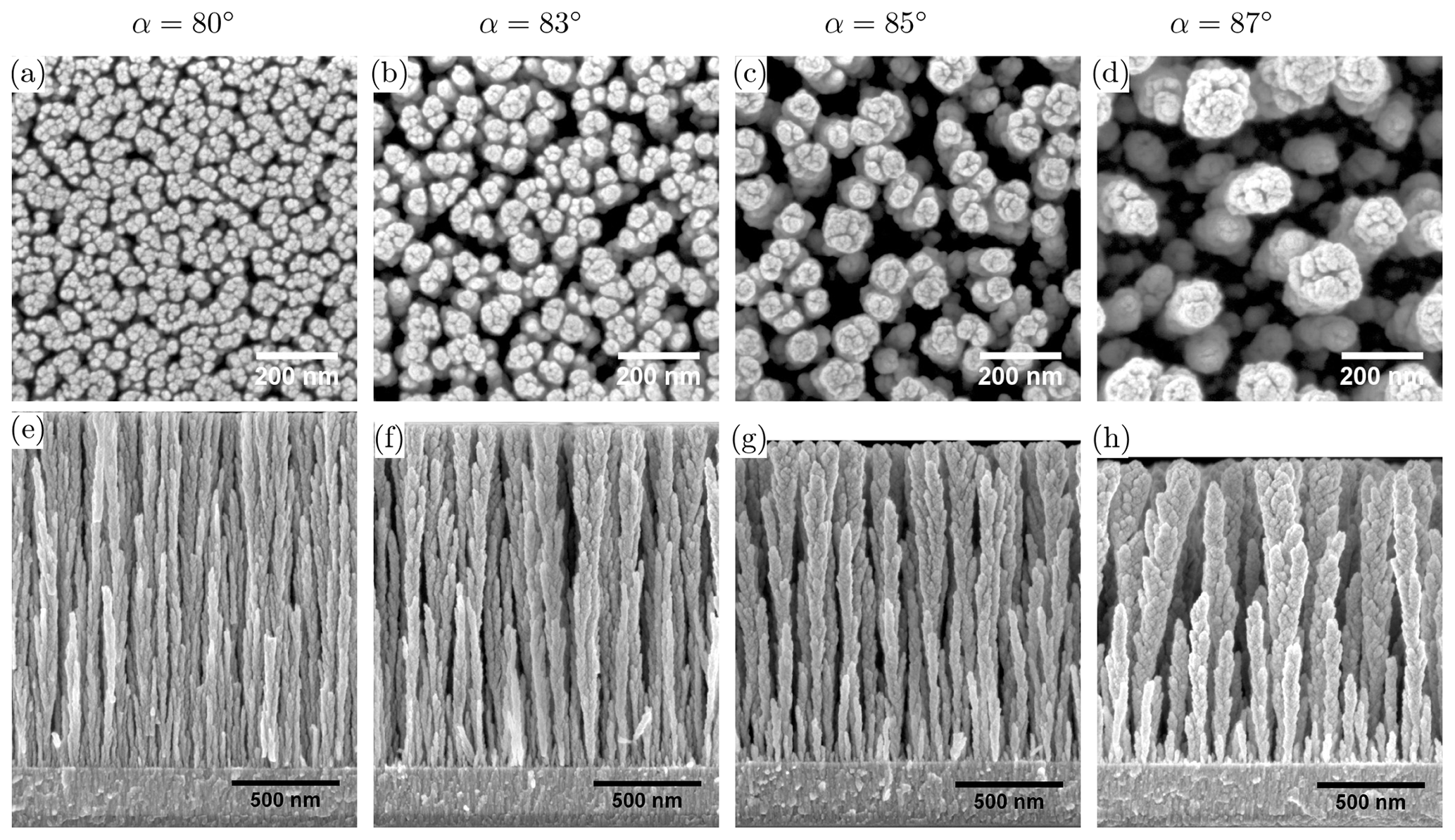
Figure 4(a)–(d) SEM top view and (e)–(h) side view images of tantalum GLAD films deposited at Pω=6.2 nm per revolution and the labeled deposition angles to produce column structures. The top-view images serve as input for the Fourier analysis.
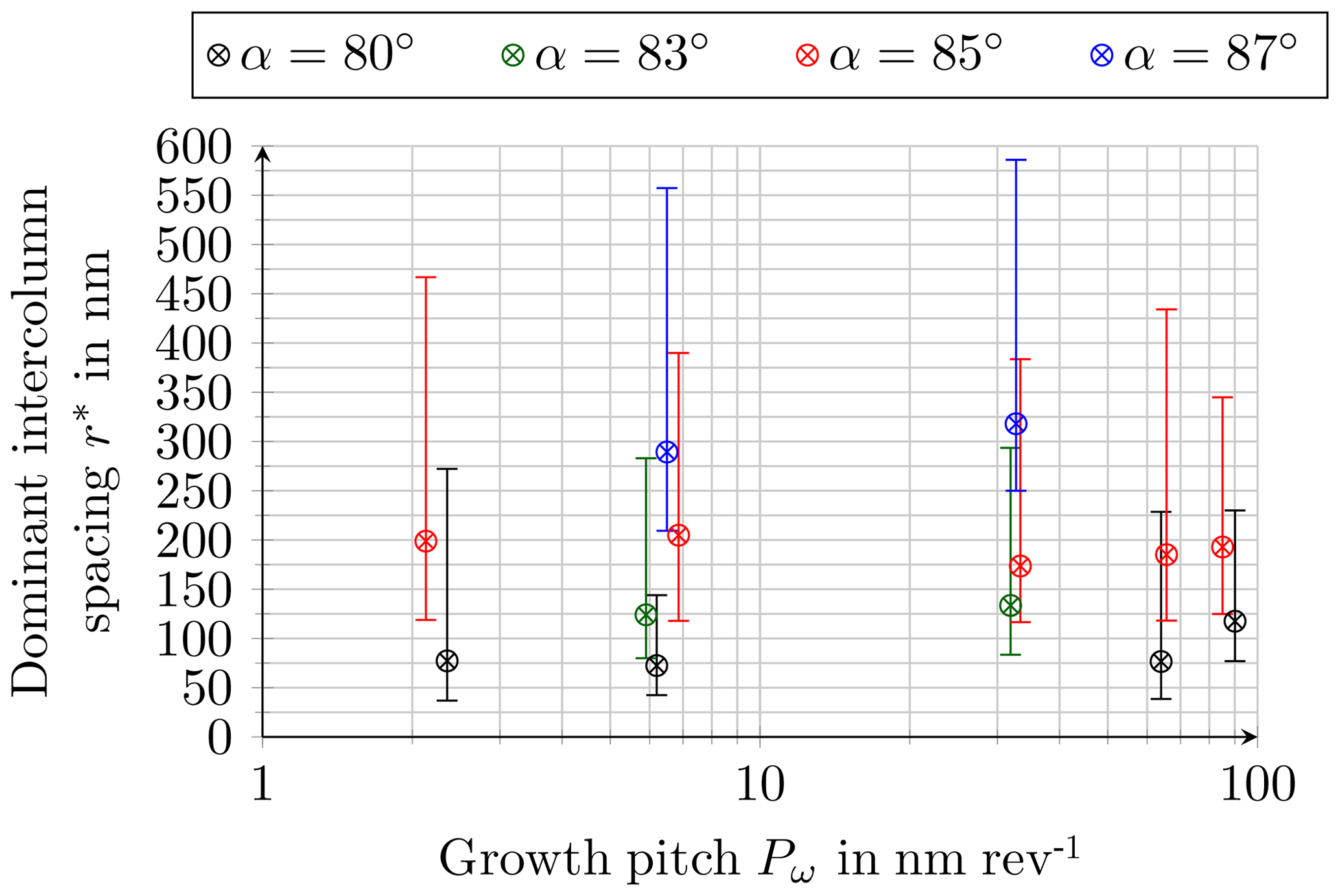
Figure 5 shows the analysis of the dominant column spacing as a function of growth pitch for the different deposition angles. For the evaluation of the dominant intercolumn spacing at the growth pitch Pω of 6.2 nm per revolution the top-view SEM images in Fig. 4 have been used. As can be seen the Fourier analysis does not produce reasonable results for the top-view SEM images of the spiral structures (Pω>170 nm per revolution). A possible explanation for this might be the insufficient resolution of the top-view SEM images of the spiral structures.
The results in Fig. 5 indicate that the dominant column spacing for α=80 and 85∘ shows only small variations depending on growth pitch. For the other deposition angles a similar tendency can be observed, but here the number of samples is too small to give a general statement. For α=85∘ the variation of the dominant column spacing as a function of growth pitch is particularly low for the screw and column structures investigated.
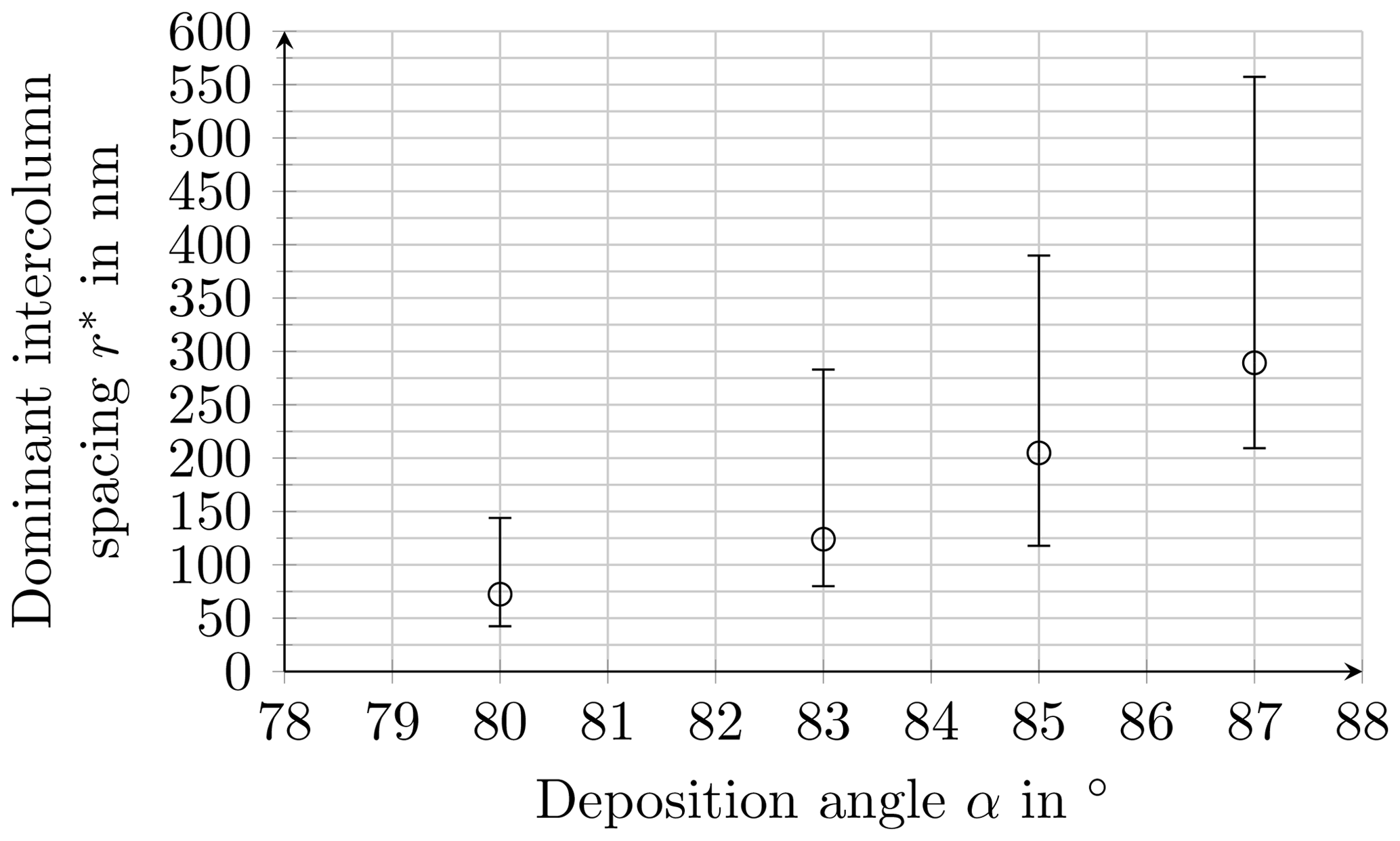
Figure 6Dominant intercolumn spacing r* versus deposition angle α. The bars show the range of variation as related to growth pitch.
With an increasing deposition angle the dominant column spacing increases strongly. At α=80∘ the mean value amounts to nm and reaches nm at α=87∘ (Fig. 6).
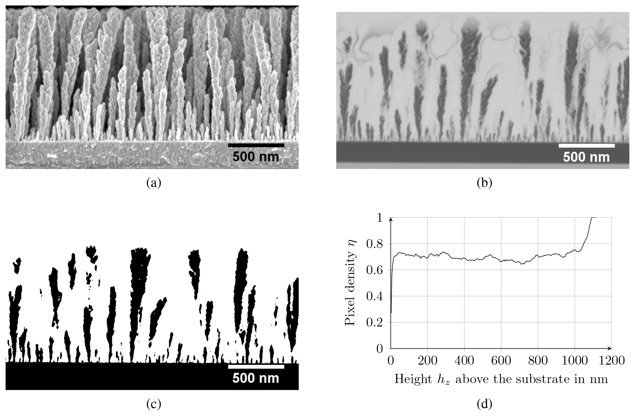
Figure 7Sample preparation to determine the pixel density dependent on the height above the substrate. (a) SEM image of the sample, (b) SEM image of the FIB sliced sample (inverted), (c) segmented FIB-SEM image, and (d) calculated pixel density from an FIB-SEM image.

Figure 8Pixel density profiles across the layer thickness for column structures (Pω=6.2 nm per revolution) at different deposition angles as a function of (a) height hz above the substrate and (b) deposition angle α. The bars indicate the variation along the height coordinate of the layer, with 95 % of the η values lying within the bars.
3.3 Porosity distribution
To reveal the cross-sectional area of the samples (Fig. 7a), a small volume is cut out by using focused ion beam (FIB) technology. The result is a smooth-cut surface that can easily be imaged with SEM. To prevent sputtering from the sample's upper part, it is covered with carbon from above. Since the SEM images have a high depth of field, the front of the sample is coated with carbon as well. The intersection surface is then polished again by an ion beam so that the carbon deposited on the interface is removed again. After such a preparation SEM images (Fig. 7b) are recorded.
Firstly, the FIB-SEM image is post-processed to separate the intersection from the image background. Due to the frontal deposition of carbon, the prepared intersection surface is distinguishable from underlying structures, which are still covered with carbon and appear darker. By applying a threshold, the intersection area can now be separated from the image (Fig. 7d). The threshold is automatically determined in Fiji using the Otsu algorithm (Otsu, 1979) to eliminate the user's subjectivity and improve reproducibility.
The pixel density η is a quality measure for the layer porosity and can be used to compare the different layers with each other. It is calculated line-by-line by counting the white pixels nW per line and putting this number in relation to the total number ntot of pixels in the latitudinal direction (Fig. 7d):
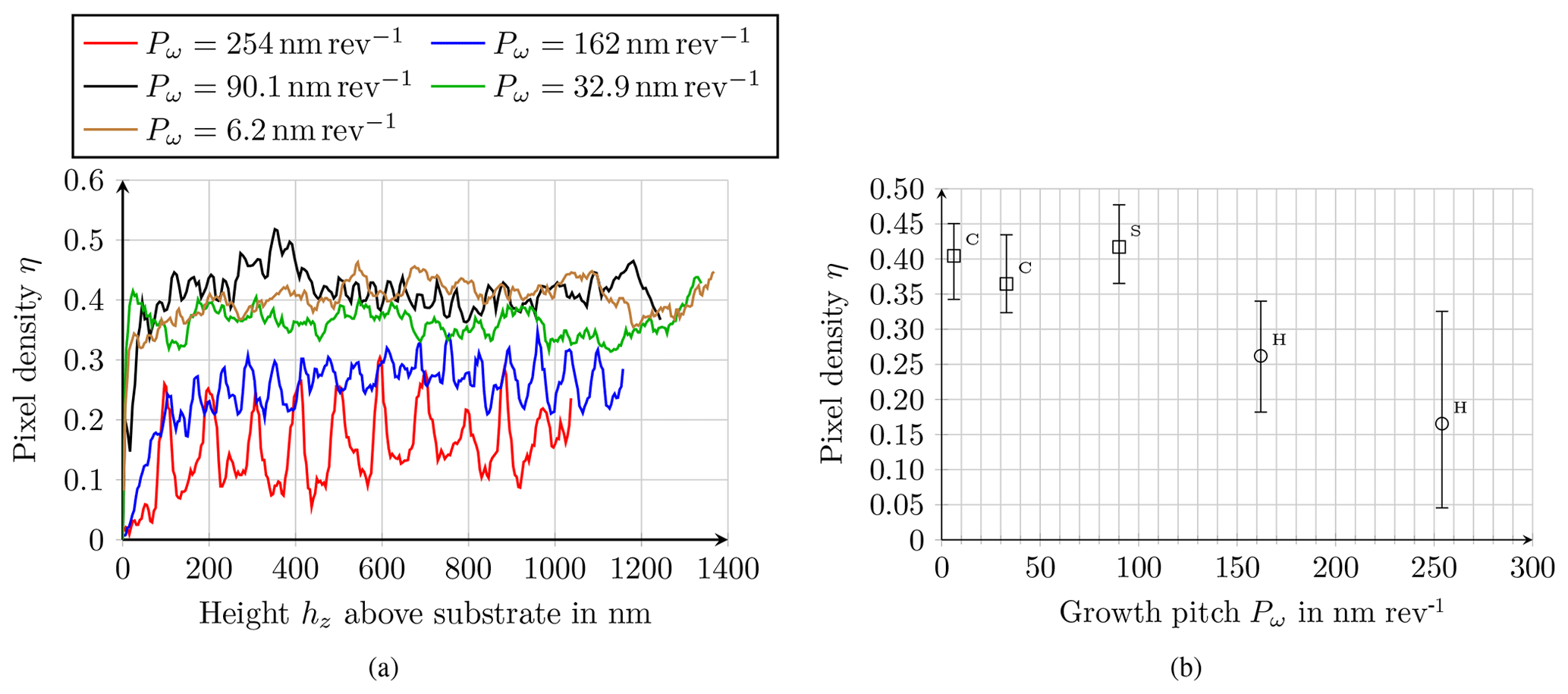
Figure 9Pixel density across the layer thickness for different layer structures with different growth pitch values Pω for a deposition angle α of 80∘ as a function of (a) height hz above the substrate and (b) pixel density η. C – columns, S – screws, H – spirals. The bars indicate the variation along the height coordinate of the layer, with 95 % of the η values lying within the bars.
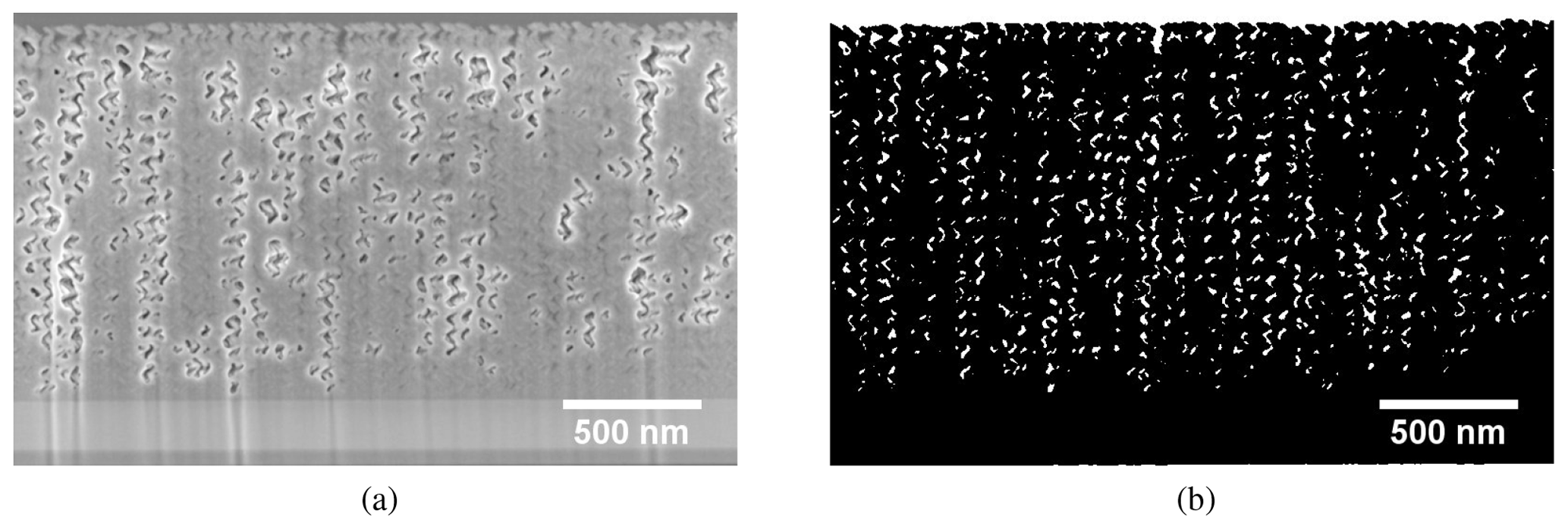
Figure 10Cross section of tantalum spiral structures deposited at α=80∘ and Pω=162 nm per revolution. (a) SEM image of the FIB-sliced sample; (b) segmented FIB-SEM image.
Plotting the pixel density of column structures (Pω=6.2 nm per revolution) as a function of height above the substrate for the different deposition angles (Fig. 8a), the ratio of material to air across the entire layer thickness is nearly constant regardless of the deposition angle. This fact confirms the assumption that the incident tantalum particles settle where they are deposited because their surface mobility is strongly limited by substrate cooling.
From Fig. 9 it becomes clear that the growth pitch, and thus the layer structure, has a significant influence on the pixel density profile. As soon as the screw structures start to transform into spirals, there is a significant reduction in η with increasing growth pitch, and the pixel density profile suddenly shows a periodic pattern. This reduction in η can be explained by the fact that the spiral structures, due to their extraordinary geometry, grow into adjacent spiral structures, which in turn produces a denser layer structure (Fig. 10).
The period of the pixel density profile seems to depend on the growth pitch. From Fig. 9 a period of approximately 100 nm at Pω=254 nm per revolution and of 66 nm at Pω=162 nm per revolution can be estimated. It is therefore assumed that the ratio of growth pitch and the period is constant:
Applying Eq. (9) to the spiral structures, it follows per revolution for Pω=254 nm per revolution and per revolution for Pω=162 nm per revolution. Under the assumption that the ratio is 2.5 per revolution, a period length of approximately 36 nm follows for a growth pitch Pω=90 nm per revolution, which means approximately five to six periods for each 200 nm interval in Fig. 9a. Counting the peaks in the 200 nm intervals in Fig. 9a, one can actually obtain this value between 5 and 6. For the column-like structures with Pω≈33 per revolution a period length of ca. 13 nm follows, which means approximately 15 periods per 200 nm interval. This large number of periods can no longer be resolved from the pixel density curve.
The following conclusions can be drawn from the experiments on the deposition of tantalum on cooled planar substrates using glancing angle deposition at different deposition angles α=(80 … 87)∘ and different growth pitches Pω≈(2 … 243) nm per revolution.
-
The thin film morphology is strongly influenced by the growth pitch. For a deposition angle α of 80∘ columns are formed with a growth pitch Pω of less than 30 nm per revolution. If the growth pitch rises above a value of 65 nm per revolution, this column structure changes to a screw structure. The shift of the layer structure towards spirals takes place in the range of Pω≈(170 … 90) nm per revolution so that for Pω>170 nm per revolution only spiral-shaped structures are formed during deposition.
-
A low growth pitch produces column structures for all deposition angles in the studied range. For these structures it is shown that the dominant spacing between the structures rises strongly with increasing deposition angle because the shadowing mechanism causes an intensified extinction of adjacent structures. At α=80∘ the mean value of the intercolumn spacing r* amounts to ca. 80 nm and rises to 205 nm at α=85∘ and 289 nm at α=87∘. These values are well comparable to the values given in the literature. Gonzalez-Garcia et al. (2012) analyzed the distribution and porosity of TiO2 layers with a height of 600 nm. The dominant column spacing was found to be ca. 124 nm at α=80∘ and 227 nm at α=85∘ (Gonzalez-Garcia et al., 2012).
-
The dominant spacing between the structures varies only slightly depending on the growth pitch. For spiral structures no conclusion can be drawn in this regard.
-
FIB-SEM images of the cross-sectional area of column structures show that the pixel density is nearly constant over the film thickness and rises with increasing deposition angle. Both findings are consistent with the results of Dick et al. (2003). By using a three-dimensional ballistic simulator it could be shown that the density of aperiodic column structures is almost constant over the column height and decreases with increasing deposition angle. Thus, the porosity rises with increasing deposition angle. The pixel densities of columns are ca. 40 % at α=80∘ and ca. 61 % at α=85∘. These values are again well comparable to the values given in the literature. Krause et al. (2011) studied thresholded top-view SEM images of GLAD columns made of TiO2 and SiO2 with a column height of about 1500 nm. For a deposition angle α of 80∘ a bulk-to-pore ratio δ of ca. 65 % was found, which corresponds to a pixel density η of ca. 60 % (). For α=85∘ the bulk-to-pore ratio is ca. 55 %, which results in a pixel density of ca. 65 %. In Gonzalez-Garcia et al. (2011, 2012) the authors used water absorption isotherms to determine the pore volume of TiO2 GLAD thin films. For a deposition angle α of 80∘ a pore volume of 58 % and for α=85∘ a pore volume of 67 % have been found.
The analysis of the influence of the growth pitch on the pixel density at a deposition angle α of 80∘ shows that a strong pixel density reduction occurs when the structures change from screws to spirals. Furthermore, the pixel density profiles of the spirals suddenly show a periodic pattern, while the period of the profile seems to depend on the growth pitch so that the ratio of the growth pitch and the period is constant; see Eq. (9).
Data are available upon request.
TO planned and performed all the experiments, carried out data processing and analysis, and drafted the paper. GG contributed to conceptualization, funding acquisition, project administration, supervision and editing.
The authors declare that they have no conflict of interest.
The authors would like to thank Alexander Tahn from the cfaed/Dresden Center for Nanoanalysis (DCN) very much for the preparation of the SEM and FIB-SEM images.
This research has been supported by the German Research Foundation (DFG) (grant no. GE 779/32) and the Open Access Publication Funds of the SLUB/TU Dresden.
This paper was edited by Ulrich Schmid and reviewed by three anonymous referees.
Albrecht, O., Zierold, R., Patzig, C., Bachmann, J., Sturm, C., Rheinländer, B., Grundmann, M., Görlitz, D., Rauschenbach, B., and Nielsch, K.: Tubular magnetic nanostructures based on glancing angle deposited templates and atomic layer deposition, Physica Status Solidi (b), 247, 1365–1371, https://doi.org/10.1002/pssb.200945560, 2010. a
Alouach, H., Fujiwara, H., and Mankey, G. J.: Magnetocrystalline anisotropy in glancing angle deposited Permalloy nanowire arrays, J. Vacuum Sc. Technol. A, 23, 1046, https://doi.org/10.1116/1.1938978, 2005. a
Beckers, N., Taschuk, M., and Brett, M.: Selective room temperature nanostructured thin film alcohol sensor as a virtual sensor array, Sensors Actuat. B, 176, 1096–1102, https://doi.org/10.1016/j.snb.2012.09.041, 2013. a
Blevin, W. R. and Geist, J.: Influence of Black Coatings on Pyroelectric Detectors, Appl. Optics, 13, 1171, https://doi.org/10.1364/ao.13.001171, 1974. a
Bruggeman, D. A. G.: Berechnung verschiedener physikalischer Konstanten von heterogenen Substanzen. I. Dielektrizitätskonstanten und Leitfähigkeiten der Mischkörper aus isotropen Substanzen, Ann. Phys., 416, 636–664, https://doi.org/10.1002/andp.19354160705, 1935. a
Budzier, H. and Gerlach, G.: Thermal Infrared Sensors: Theory, Optimisation and Practice, John Wiley & Sons Ltd, Chichester, West Sussex, UK, https://doi.org/10.1002/9780470976913.ch6, 2011. a, b
Buzea, C., Beydaghyan, G., Elliott, C., and Robbie, K.: Control of power law scaling in the growth of silicon nanocolumn pseudo-regular arrays deposited by glancing angle deposition, Nanotechnology, 16, 1986–1992, https://doi.org/10.1088/0957-4484/16/10/002, 2005. a
Dice, G. D., Brett, M. J., Wang, D., and Buriak, J. M.: Fabrication and characterization of an electrically variable, nanospring based interferometer, Appl. Phys. Lett., 90, 253101, https://doi.org/10.1063/1.2749418, 2007. a
Dick, B., Brett, M. J., and Smy, T.: Controlled growth of periodic pillars by glancing angle deposition, J. Vacuum Sci. Technol. B, 21, 23–28, https://doi.org/10.1116/1.1529652, 2003. a
Garnett, J. C. M.: Colours in Metal Glasses and in Metallic Films, Philos. T. Roy. Soc. A, 203, 385–420, https://doi.org/10.1098/rsta.1904.0024, 1904. a
Garnett, J. C. M.: Colours in Metal Glasses, in Metallic Films, and in Metallic Solutions. II, Philos. T. Roy. Soc. A, 205, 237–288, https://doi.org/10.1098/rsta.1906.0007, 1906. a
Gonzalez-Garcia, L., Gonzalez-Valls, I., Lira-Cantu, M., Barranco, A., and Gonzalez-Elipe, A. R.: Aligned TiO2 nanocolumnar layers prepared by PVD-GLAD for transparent dye sensitized solar cells, Energ. Environ. Sci., 4, 3426, https://doi.org/10.1039/C0EE00489H, 2011. a, b
Gonzalez-Garcia, L., Parra-Barranco, J., Sanchez-Valencia, J. R., Barranco, A., Borras, A., Gonzalez-Elipe, A. R., Garcia-Gutierrez, M.-C., Hernandez, J. J., Rueda, D. R., and Ezquerra, T. A.: Correlation lengths, porosity and water adsorption in TiO2 thin films prepared by glancing angle deposition, Nanotechnology, 23, 205701, https://doi.org/10.1088/0957-4484/23/20/205701, 2012. a, b, c
Hawkeye, M. M. and Brett, M. J.: Glancing angle deposition: Fabrication, properties, and applications of micro- and nanostructured thin films, J. Vacuum Sci. Technol. A, 25, 1317, https://doi.org/10.1116/1.2764082, 2007. a
Hawkeye, M. M., Taschuk, M. T., and Brett, M. J.: Glancing Angle Deposition of Thin Films, John Wiley & Sons Ltd, Chichester, West Sussex, UK, https://doi.org/10.1002/9781118847510, 2014. a, b
Hwang, S., Kwon, H., Chhajed, S., Byon, J. W., Baik, J. M., Im, J., Oh, S. H., Jang, H. W., Yoon, S. J., and Kim, J. K.: A near single crystalline TiO2nanohelix array: enhanced gas sensing performance and its application as a monolithically integrated electronic nose, Analyst, 138, 443–450, https://doi.org/10.1039/c2an35932d, 2013. a
Kennedy, S. R., Brett, M. J., Toader, O., and John, S.: Fabrication of Tetragonal Square Spiral Photonic Crystals, Nano Lett., 2, 59–62, https://doi.org/10.1021/nl015635q, 2002. a
Kennedy, S. R., Brett, M. J., Miguez, H., Toader, O., and John, S.: Optical properties of a three-dimensional silicon square spiral photonic crystal, Photon. Nanostruct.-Fundament. Appl., 1, 37–42, https://doi.org/10.1016/s1569-4410(03)00005-1, 2003. a
Krause, K. M., Thommes, M., and Brett, M. J.: Pore analysis of obliquely deposited nanostructures by krypton gas adsorption at 87 K, Micropor. Mesopor. Mater., 143, 166–173, https://doi.org/10.1016/j.micromeso.2011.02.023, 2011. a
Landauer, R.: Electrical conductivity in inhomogeneous media, in: AIP Conference Proceedings, Vol. 40, 7–9 September 1977, Columbus, OH, USA, edited by: Garland, J. C. and Tanner, D. B., https://doi.org/10.1063/1.31150, ISBN 0-88318-139-8, 1978. a
Otsu, N.: A Threshold Selection Method from Gray-Level Histograms, IEEE T. Syst. Man Cybernet., 9, 62–66, https://doi.org/10.1109/tsmc.1979.4310076, 1979. a
Robbie, K.: Advanced techniques for glancing angle deposition, J. Vacuum Sci. Technol. B, 16, 1115, https://doi.org/10.1116/1.590019, 1998. a, b
Robbie, K., Friedrich, L. J., Dew, S. K., Smy, T., and Brett, M. J.: Fabrication of thin films with highly porous microstructures, J. Vacuum Sci. Technol. A, 13, 1032–1035, https://doi.org/10.1116/1.579579, 1995. a
Schindelin, J., Arganda-Carreras, I., Frise, E., Kaynig, V., Longair, M., Pietzsch, T., Preibisch, S., Rueden, C., Saalfeld, S., Schmid, B., Tinevez, J.-Y., White, D. J., Hartenstein, V., Eliceiri, K., Tomancak, P., and Cardona, A.: Fiji: an open-source platform for biological-image analysis, Nat. Meth., 9, 676–682, https://doi.org/10.1038/nmeth.2019, 2012. a
Schossig, M.: Ultradünne, freitragende Lithiumtantalat-Elemente für hochdetektive Infrarotsensoren, dissertation, Fakultät für Elektrotechnik und Informationstechnik, TU Dresden, Dresden, 2012a. a
Schossig, M.: Optical Absorption Layers for Infrared Radiation, in: Bio and Nano Packaging Techniques for Electron Devices: Advances in Electronic Device Packaging, chap. 18, edited by: Gerlach, G. and Wolter, K. J., Springer, Berlin, Heidelberg, 355–381, https://doi.org/10.1007/978-3-642-28522-6, 2012b. a
Schossig, M., Norkus, V., and Gerlach, G.: Infrared Responsivity of Pyroelectric Detectors With Nanostructured NiCr Thin-Film Absorber, IEEE Sensors J., 10, 1564–1565, https://doi.org/10.1109/JSEN.2010.2046162, 2010. a
Singh, J. P., Tang, F., Lu, T. K. T., and Wang, G.: Enhanced cold field emission from 100 oriented β−W nanoemitters, J. Vacuum Sci. Technol. B, 22, 1048, https://doi.org/10.1116/1.1736642, 2004. a
Zhao, Y., Wang, G.-C., and Lu, T.-M.: Characterization of Amorphous and Crystalline Rough Surfaces: Principles and Applications, Elsevier, Amsterdam, https://doi.org/10.1016/s1079-4042(01)80055-2, 2001. a, b
The angular-averaged power spectral density RPSD can be calculated from the PSD image using the radial profile extended plugin.