the Creative Commons Attribution 4.0 License.
the Creative Commons Attribution 4.0 License.
 | 30 Oct 2019
Three-dimensional structural comparison of tantalum glancing angle deposition thin films by FIB-SEM
Tobias Ott
Diego Roldán
Claudia Redenbach
Katja Schladitz
Michael Godehardt
Sören Höhn
Thin tantalum films generated by glancing angle deposition serve as functional optical layers, for instance as absorption layers for ultrathin infrared sensors. They consist of nano-rods whose dimensions and distribution influence the optical properties of the thin film. Serial sectioning by a focused ion beam combined with scanning electron microscopy of the slices generates stacks of highly resolved images of this nanostructure. Dedicated image processing reconstructs the spatial structure from this stack such that 3-D image analysis yields geometric information that can be related to the optical performance.


In this paper, we investigate the nanostructure of two thin optical layers as applied in pyroelectric sensors. The samples are made of tantalum and produced using glancing angle deposition (GLAD, Robbie, 1998). Their optical properties are not only determined by those of the tantalum base material but essentially by their rod-like nanostructure. This fine structure can be imaged spatially by the combination of sequential slicing by a focused ion beam (FIB) and imaging by scanning electron microscopy (SEM). As the tantalum GLAD samples are highly porous, reconstructing their spatial structure from the raw FIB-SEM image stack requires high image processing effort. We report the complete image processing pipeline developed for this purpose. Finally, we measure various geometric characteristics describing the shape and arrangement of the nano-rods as functions of height over the substrate.
The thermal resolution of a pyroelectric sensor is directly proportional to the absorption of the sensor element (Budzier and Gerlach, 2011, p. 118) – therefore, the absorption should be as high as possible. An optimal absorption layer is characterized by a spectrally uniform high absorption and a low heat capacity (Blevin and Geist, 1974; Schossig, 2012b). Schossig et al. (2010) used GLAD to produce such an absorption layer of nichrome (NiCr) that strongly increased the spectral responsivity of a pyroelectric sensor.
GLAD is a special physical vapor deposition process (PVD) for thin films. It features the deposition under grazing incidence with very high deposition angles () and substrate rotation. By rotating and tilting the substrate at a certain deposition angle, nanostructures grow on the substrate and form a porous layer. The shape and spacing of these structures can be influenced by the deposition parameters (Robbie et al., 1995; Robbie, 1998).
The use of GLAD is not limited to optical functional layers. It has also been applied in photonic crystals (Kennedy et al., 2002, 2003), gas sensors (Hwang et al., 2013; Beckers et al., 2013), field emitters (Singh et al., 2004), nanomechanical actuators (Dice et al., 2007), and magnetic devices (Albrecht et al., 2010; Alouach, 2005), to name a few.
We study two absorption layers, which are deposited under rapid rotation with deposition angles of and , respectively. Thus, nano-rods grow on the surface of the substrate. The dimensions and spatial distribution of the nano-rods influence the optical properties of the thin film and depend strongly on the deposition angle (Hawkeye and Brett, 2007, p. 1322). Variations in this angle lead to changes in the porosity of the thin film. Therefore, a structural analysis is essential to quantify these changes and to determine the optical properties of the resultant porous layers.
Three-dimensional (3-D) image data allow for truly spatial structural characterization. In particular, pore and particle sizes can be analyzed without strong assumptions regarding the shape. Moreover, preferred directions, spatial arrangement, and connectivity can only be analyzed based on 3-D images. For structures finer than 100 nm, FIB-SEM is the imaging method of choice. For recent reviews of this 3-D imaging technique as well as microstructure characterization and simulation for porous ceramics we refer to Holzer et al. (2016); Penner and Holzer (2018); Prill et al. (2019). However, in particular for highly porous materials, FIB-SEM causes several typical imaging artifacts, see Bassim et al. (2012), Joos et al. (2011), Tomus and Pang (2013), Prill et al. (2013) and Fitschen et al. (2017).
Here, severe curtaining is the dominant problem. These artifacts are due to inexact planar slicing by the FIB and appear as stripes in the vertical (slicing) direction. They can be removed by filtering in Fourier space (see Liu et al., 2018 and Schankula et al., 2018), filtering the vertical component of a wavelet decomposition (as devised by Münch et al., 2009), and variational methods (described by Fehrenbach et al., 2012 and Fitschen et al., 2017). Here, we face curtaining in the same size range as the actual structure. Moreover, the structure itself is elongated in the vertical direction. Thus, all of these “decurtaining” methods distort the structure. Therefore, we use a new approach, tailor-suited to the special features of the investigated optical layer.
Additionally, FIB-SEM images of highly porous structures contain so-called shine-through artifacts (Prill et al., 2013), consisting of structures belonging to deeper slices that are visible in the current slice. Thus, the segmentation of highly porous structures is not straightforward. Several segmentation algorithms (Prill et al., 2013, 2019; Salzer et al., 2015) are dedicated to overcoming these artifacts. Here, we apply a new approach to deal with them.
Finally, we analyze the reconstructed structures concerning porosity, anisotropy, and layering. To this end, we measure porosity; the mean chord lengths, which determine structural elongation in a given direction; and the spherical contact distribution. The latter is a versatile tool for characterizing complex structures (e.g., Ohser and Schladitz, 2009; Stenzel et al., 2014; Machado et al., 2018) and provides information about how regular or disordered the investigated structure is, in addition to other important details.
FIB-SEM imaging has successfully been used to study properties of a single nano-rod as a function of film thickness for porous titanium oxide (titania, TiO2) film obtained by GLAD (see, e.g, Krause et al., 2010). Additionally, in Krause et al. (2011) pores are characterized by gas absorption and image analysis techniques determining mean distances between TiO2 columns. In this paper, we investigate the resultant porous structures obtained by the selected deposition angles to quantitatively compare both thin films. To our knowledge, this is the first study of its kind. The results will help to better understand the relation of deposition parameters and optical properties of GLAD thin films. The first step to link the optical properties of the thin film with the deposition parameters is to determine the porosity distribution over the film thickness as shown in this publication. In a subsequent step, which goes beyond the scope of this paper, the optical properties (e.g., the spectral absorption coefficient) can be calculated from the porosity distribution using the effective medium theory (Bruggeman, 1935; Garnett, 1904, 1906). Thus, it is possible to produce absorption layers with tailored optical properties for thermal infrared detectors that exhibit high absorption in the desired spectral range and low heat capacity. As a result, the spectral responsivity of such sensors can be improved.
This paper is organized as follows. Sections 2 and 3 present the preparation and imaging of the absorption layers. Section 4 is dedicated to image processing and reconstruction of the solid phase. Section 5 contains the structural analysis. Conclusions are given in Sect. 6.
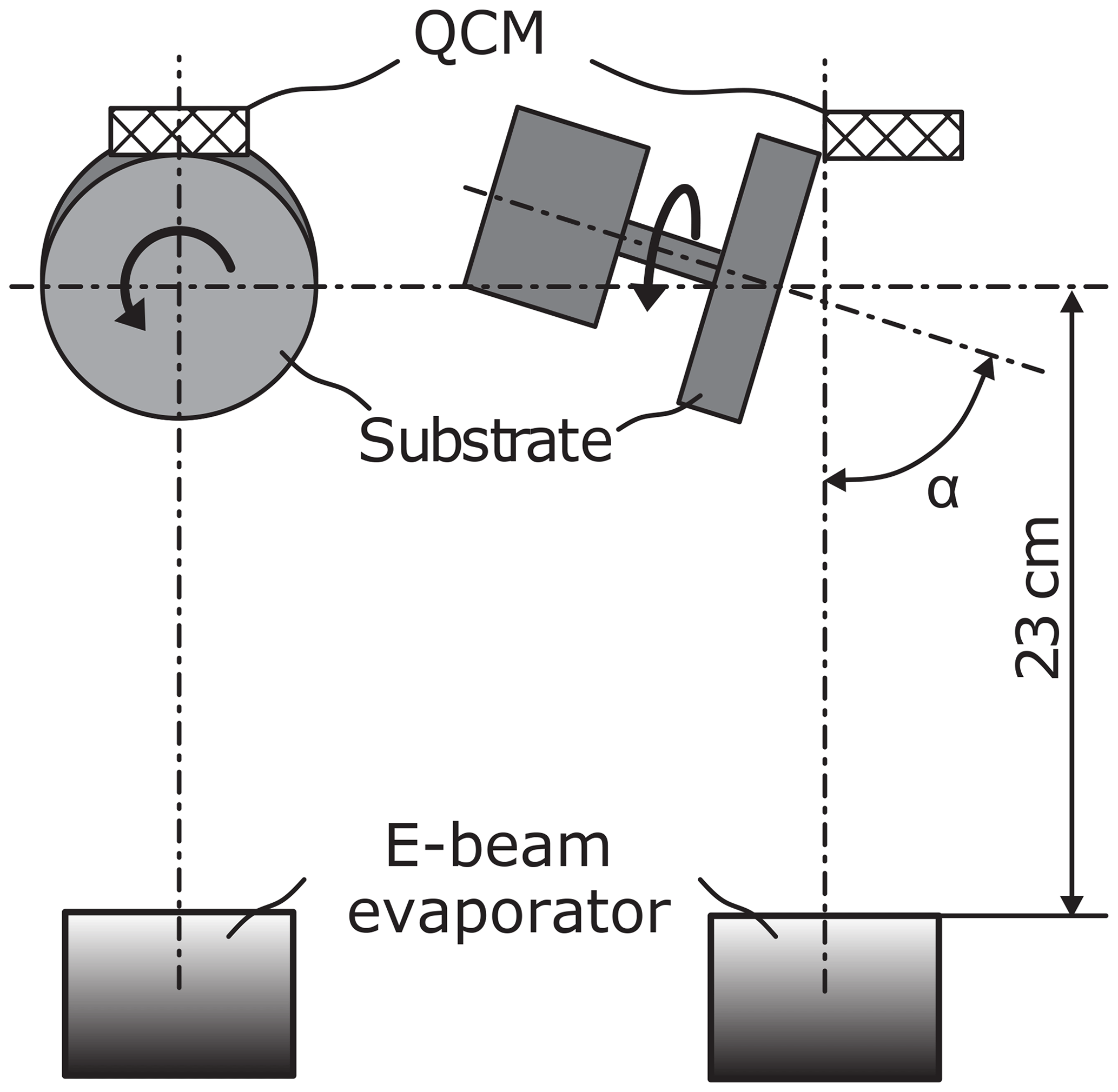
A schematic representation of the setup of the deposition system is presented in Fig. 1. The tantalum target is heated with an electron beam evaporator and transferred into the gas phase. The distance between the target and the substrate is 23 cm. The substrate is tilted at deposition angle α and is rotated rapidly at 10.5 rev min−1. The deposition rate is monitored and kept constant during the entire deposition process using a quartz crystal monitor placed at a fixed position in the vacuum chamber.
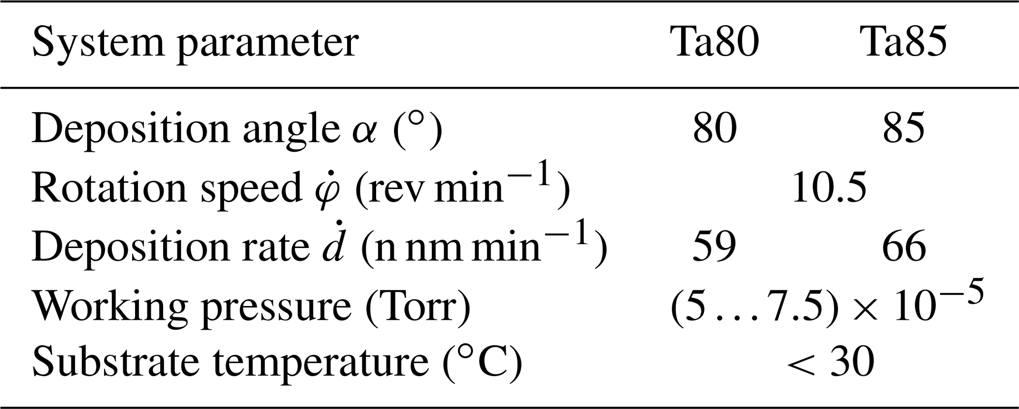
We investigate two absorption layers – Ta80 and Ta85 – which have the following respective deposition angles: and . Table 1 summarizes the conditions used for the deposition of these samples.
A substrate temperature above 30 % of the melting temperature of the target material increases the surface mobility of the impinging particles. In this case, the substrate temperature can be regarded as a further degree of freedom to influence the film structure (Hawkeye et al., 2014, p. 73). To reduce the degrees of freedom and for better reproducibility, the substrate is cooled actively so its temperature is held below 30 ∘C during the evaporation. As a result, the diffusion length of the adsorbed particles on the substrate surface is reduced to a negligible level. The tantalum was deposed at a working pressure of – Torr.
Table 1Conditions for the deposition of the Ta80 and Ta85 samples.
FIB-SEM measurements are conducted using the Crossbeam NVision 40 field emission scanning electron microscope (FE-SEM) by Carl Zeiss with integrated advanced tomography package Atlas 5 3-D-Tomography. This equipment allows for high-resolution 3-D images with defined pixel sizes in all directions to be recorded.
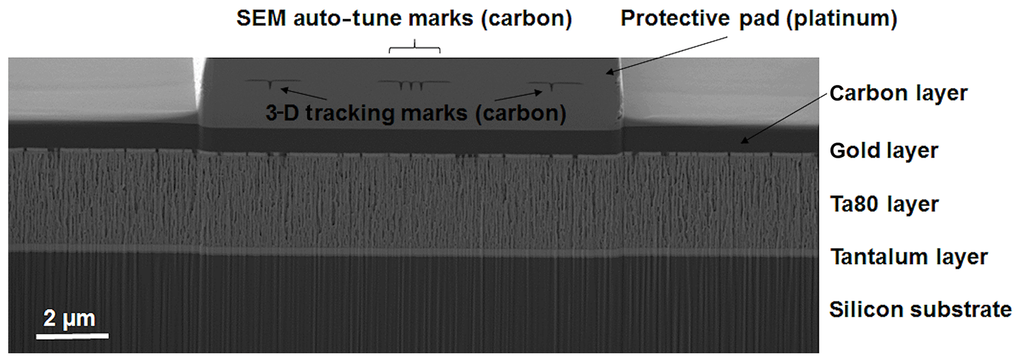
For minimization of charging effects and sample drift during the long measurement period, the sample is first fixed and electrically conducted by conductive silver. In addition, the whole sample surface is coated by an approximately 100 nm thick gold layer. For the protection of the 3-D preparation area and to ensure sharp-edge FIB cuts, an approximately local carbon layer is applied by ion beam deposition.
Finally, a platinum layer with carbon marks is deposited for automated slice thickness control, auto-focus, and auto-stigmation functions using the SEM “AutoTune” and “3-D Tracking Marks” tools from the Zeiss Atlas 5 software (Carl Zeiss Microscopy, 2019). A cross-section of the final, prepared Ta80 sample is shown in Fig. 2.
For the Ta80 and Ta85 samples, respective data sets of 500 and 700 (3800 pixel × 1480 pixel) SEM slices are captured at a resolution of . The FIB/SEM parameters are adapted manually and optimized for the tantalum as there are no standard conditions for FIB/SEM. In particular, parameters have to be optimized for the dissipation of the electric charge introduced by the electron beam and for reducing sample charging and sample drift so that the sample remains constant under the electron beam for hours. Thus, for the tantalum samples, the SEM is operated at a 2 keV acceleration voltage, and the FIB current is 1.5 nA with a slice thickness resolution of 10 nm. For all experiments, the secondary electron (SE) and the Inlens SE detectors are applied simultaneously. Both samples are imaged under the same conditions to ensure comparability. The images show not only the material to be analyzed but also the surroundings; thus, the segmentation is performed on a subset of the data sets referred to as the region of interest.
For the reconstruction of the porous 3-D structure, only the secondary electron (SE) images are used due to their superior gray value contrast compared with the Inlens SE detector images.
Throughout the paper, the following coordinate system is used: the x direction is parallel to the substrate, the y direction is parallel to the nano-rods' growth, and the z direction corresponds to the stacking direction.
Figure 3 shows representative slices of the samples. The Ta80 data set (Fig. 3a) is strongly compromised by curtaining artifacts in the same size range as the structure. Thus, decurtaining is indispensable in this sample. The Ta85 data set (Fig. 3b) also features curtaining artifacts. However, they have less impact due to the coarser structure and, therefore, do not need special attention.
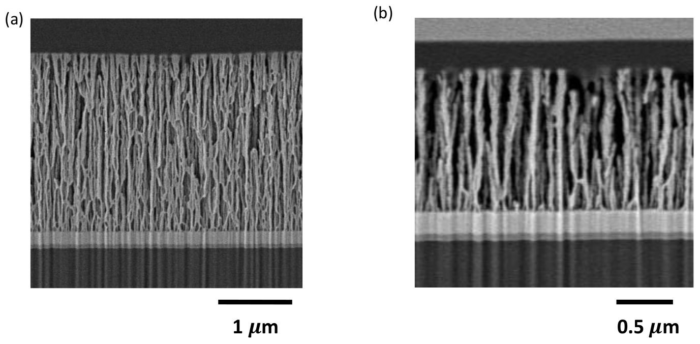
In addition to being coarser, Ta85 is more porous. Therefore, shine-through artifacts are present in this sample. Algorithms to reconstruct the structure in spite of these artifacts are available (Prill et al., 2013; Salzer et al., 2015). Nevertheless, these algorithms require several parameters and can introduce artificial anisotropy as they were devised to detect features along the z direction.
Thus, we exploit the elongated pore shape in the Ta85 sample to introduce an alternative method that can extract the shine-through artifacts, allowing reconstruction by global thresholding.
4.1 Preprocessing
First, the images are aligned using ImageJ's StackReg plugin as described by Thevenaz et al. (1998). StackReg aligns by propagating the image information from one slice to the next causing a parallelogram distortion in the yz plane that is subsequently corrected by ImageJ's TransformJ from Meijering et al. (2001). This results in 1001 pixels × 289 pixels × 390 pixels with a size of , corresponding to a sample size of for sample Ta80. For sample Ta85, we get 597 pixels × 146 pixels × 59 pixels with a size of , corresponding to a sample size of .
Later, we apply a gray value normalization on both samples to correct illumination gradients as follows: first, we compute the mean gray value along all x rows; then we subtract the resulting mean yz slice from all yz slices to reduce global gray value fluctuations in the y and z directions; and, finally, we repeat this procedure for the z columns to ameliorate the gray values in the x and y directions.
4.2 Reconstruction of sample Ta80
For Ta80, a dedicated decurtaining algorithm is needed as state-of-the-art methods (Münch et al., 2009; Fitschen et al., 2017; Liu et al., 2018) fail due to the singular vertical shape of the structure and pores, which are in the same size range. Our method thrives on the layered structure of the sample, resulting in three regions of interest in the image: the top of the slices, which is free of curtaining; the central region holding the porous structure with curtaining artifacts; and the bottom region with curtaining artifacts and with similar gray values to the top region.
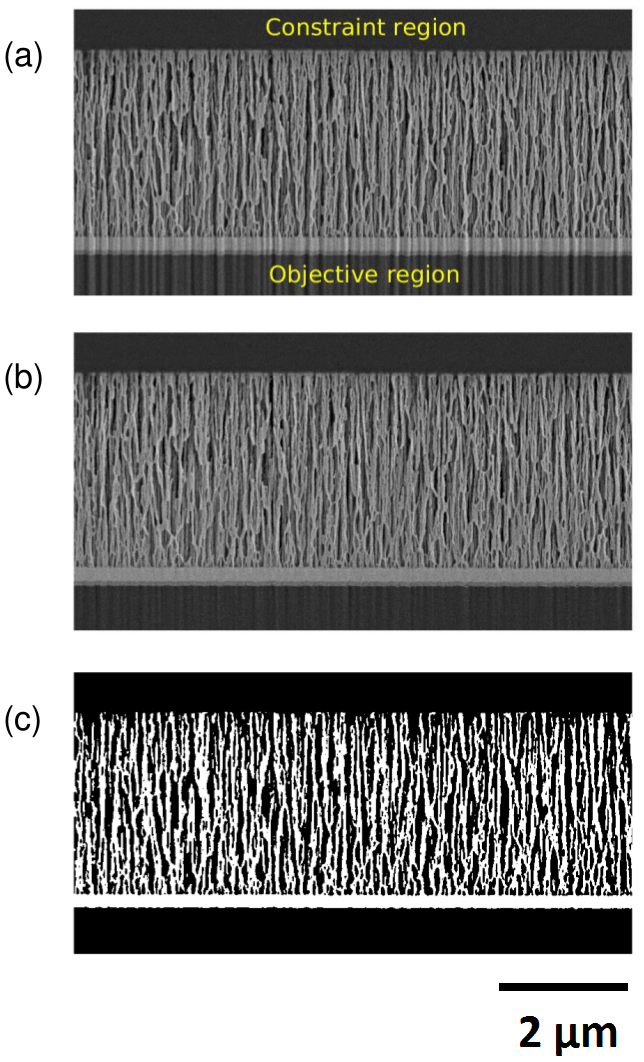
Figure 4Decurtaining of Ta80. A slice from the original Ta80 sample showing the objective and constraint regions (a). The slice after the decurtaining algorithm (b) and binarization (c).
More precisely, from the bottom to top in the y direction, we have the silicon substrate, the solid tantalum layer, the porous tantalum forming the actual optical layer, the sputtered gold layer, and, finally, the carbon layer (see Fig. 2). As it is on the top, the carbon layer is not affected by curtaining (see Fig. 4a). The gray values of the carbon layer and the silicon substrate are nearly equal, as silicon and carbon are both nonmetallic elements with almost the same density. Thus, our decurtaining algorithm proceeds as follows:
-
A region of interest (ROI) is cropped, as shown in Fig. 4a. This ROI should contain the top and bottom regions with equal or similar intensity (carbon and silicon layers).
-
The top layer (without curtaining) is selected as a constraint region, and the bottom layer (with curtaining) is selected as an objective region.
-
The curtaining artifacts are then removed column-wise by the next two steps:
- a.
compute the gray value means mc and mo for the constraint and objective regions within the current column;
- b.
add mc−mo to all pixel gray values in the current column.
- a.
If the current column features a dark artifact, then mc>mo and the correction increases the gray values in the column. If the current column features a bright artifact, then mc<mo and the correction decreases the gray values in the column. The ROI selected in the first step of the algorithm is the same as that described above at the end of the Sect. 3. The results are shown in Fig. 4b.
The decurtained sample Ta80 is directly reconstructed using global thresholding (Fig. 4c). We choose the threshold value manually such that the typical shape of the nano-rods (as narrow vertical structures with small embedded pores) is preserved. Figure 7a shows a volume rendering of the reconstruction.
4.3 Reconstruction of sample Ta85
Sample Ta85 is more porous and coarser than sample Ta80. Hence, global thresholding cannot be applied directly because of the shine-through artifacts. Here, we can exploit the particular elongated pore shape and structural width of the sample to remove the shine-through artifacts in a preprocessing step. This allows us to subsequently binarize by using global thresholding.
Figure 5a shows an xz slice of the Ta85 image. Here, we observe a vertical pattern of the structure, where the deep pores are identified by dark regions. Shine-through artifacts and solid phase are visible as well. However, the solid and the pore phases have nearly constant gray values, whereas shine-trough artifacts have gray values that increase vertically. Thus, we remove them by filtering as follows: we increase the visibility of edges, surface details, and reduce the noise in the images by applying a difference of Gaussians, which consists of the subtraction of two blurred images obtained by applying Gaussian blurring on the original images at specified σ2 and σ1.
This algorithm is typically applied with a size ratio of 4:1 for σ2 to σ1. Thus, the sigma sizes are and , where the first component belongs to the x direction, the second belongs to the y direction, and the third belongs to the z direction. Figure 5b shows a representative slice after filtering using difference of Gaussians.
Subsequently, we apply a morphological fill-holes operation that removes all regional minima which are not connected to the image border (Soille, 1999). The regional minima are obtained by subtracting the input stack from the stack to which fill-holes has been applied (Fig. 5c). This image shows regions that definitely belong to the pore phase in black. Still, the nonzero regions contain shine-through artifacts.
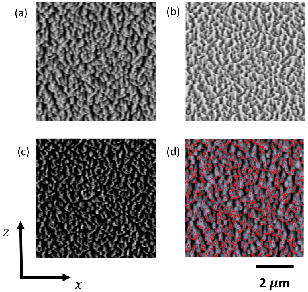
Figure 5Ta85 xz profiles: (a) the original stack, (b) after difference of Gaussians, (c) after the subtraction of fill-holes, and (d) the overlapped image (red represents the matrix phase, and blue represents the extracted shine-through artifacts).

Figure 6Reconstruction result of the Ta85 sample shown as a red overlay on the gray value slices: (a) xy direction, (b) yz direction, and (c) a close-up of the yz direction.
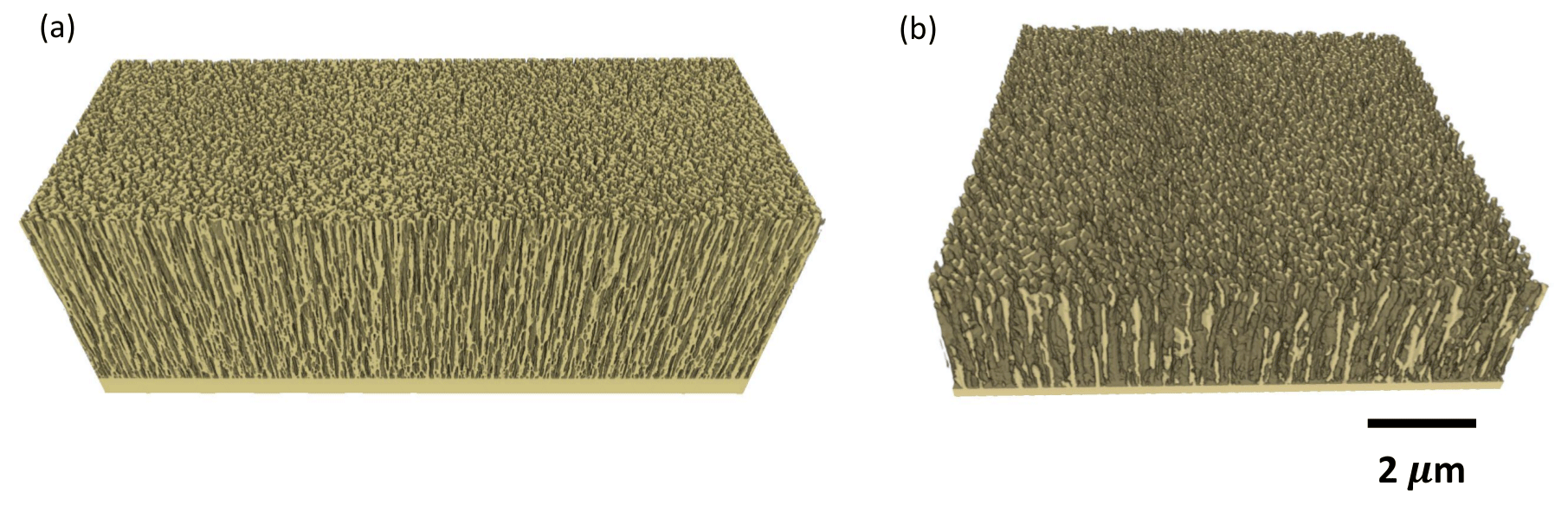
Figure 7Volume renderings of the reconstructed Ta80 and Ta85 samples. (a) Ta80: . (b) Ta85: .
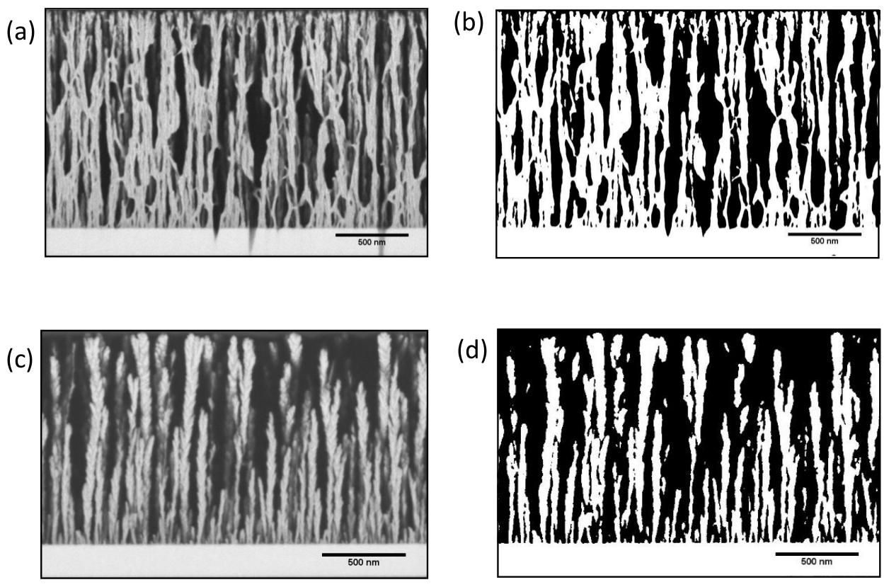
Figure 8Highly resolved SEM images and binarizations of the absorption layers. Pixel edge lengths 3 nm. (a) Sample Ta80. (b) Binarization of (a). (c) Sample Ta85. (d) Binarization of (c). The tantalum component of Ta80 appears thinner than that of sample Ta85. Moreover, pores in Ta85 grow bottom up.
We extract them using a white top-hat transform, which removes small elements and details from images given a suitable structuring element. This morphological operation considers the difference of the original image and its morphological opening. The structuring element for the opening can be chosen according to the shape of the artifacts, which are extended in the z direction. A cuboid of size has given good results for the extraction of the artifacts. Figure 5d shows shine-through artifacts (blue) and the solid phase (red) overlapped.
After removing the shine-through artifacts, the images are segmented by global gray value thresholding with a manually chosen threshold. See Fig. 6 for the results. A volume rendering of the reconstructions is show in Fig. 7b.
4.4 Porosity validation
We use highly resolved 2-D images of the Ta80 and Ta85 samples with a 3 nm × 3 nm pixel size to validate our reconstructions regarding the porosity. The samples considered here belong to smaller thin films deposited with the same conditions as those presented above. For sample Ta80, the maximum height of the smaller version is 1400 nm. We denote this sample as Ta80a.
Figure 8a and c show these highly resolved 2-D images. They are segmented by applying a manually chosen global threshold as shown in Fig. 8b and d. Porosities regarding the height of these images are shown in Fig. 9a. Here, a height of 0 nm represents the height at which the substrate ends. Figure 9b shows the mean porosity in xz slices along the height y for the 3-D case.
For sample Ta80, the porosity of the highly resolved 2-D image varies (40 %±9 %), whereas the average porosities of the 3-D case are around 48 %, i.e., the porosities are consistent. For sample Ta85, the porosity in the 2-D case remains around 61 %±5 % for low to middle heights, while for high heights the porosity increases. In the 3-D case, the average porosity stays close to 65 % with a tendency to increase with the height following the previously described trend.

Figure 9Porosities as functions of the height over the substrate: (a) Porosity in 1-D segments of the 2-D images from Fig. 8b and d. (b) Porosity in xz slices of the reconstructed FIB-SEM stacks. Porosity remains nearly constant for Ta80, whereas it increases with height for Ta85.
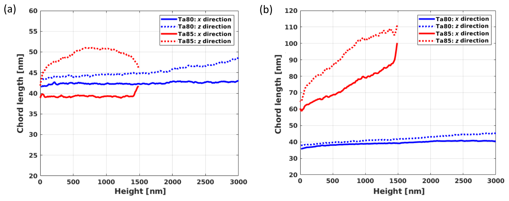
Figure 10Slice-wise mean chord lengths in the x and z directions as functions of the height above the substrate for the solid phase and pore phase of the reconstructed FIB-SEM stacks: (a) solid phase and (b) pore phase. For Ta80, mean chord lengths do not vary strongly. Only the solid phase tends to be more elongated in the z direction with increasing height. For Ta85, both the solid phase and the pore phase are elongated in the z direction. Moreover, pore sizes clearly grow with height.
Porosity provides a first insight concerning structural differences between the samples. Indeed, Fig. 9b shows that sample Ta80 is less porous than sample Ta85 (by nearly 20 %) with a noticeable increase with height. Nevertheless, this measure is insufficient for sample characterization. To quantitatively measure both samples, we determine the mean thickness and the mean pore size at different heights above the substrate. For this reason, we compute the mean chord lengths for the solid and pore phases. The mean chord length is the expectation of the length of the typical chord obtained when intersecting the structure with lines in a given direction (see e.g., Ohser and Schladitz, 2009). Elongated structures have a larger mean chord length in the direction of their elongation.
In particular, we study the mean chord lengths in the x and z directions as functions of the heights as show Fig. 10a and b. For sample Ta80, the mean chord lengths tend to be stable in the sense that they remain in the 42±10 nm and 38±10 nm intervals for the solid phase and pore phase, respectively. Conversely, for sample Ta85, the mean chord lengths of the pore phase increase with height as shown in Fig. 10b.
Furthermore, in both samples, we observe an artificial anisotropy. More precisely, the mean chord lengths in the x and z directions should be equal but differ by almost 7 % and 18 % for Ta80 and Ta85, respectively. For sample Ta80, this is due to imperfectly removed curtaining biasing the chord lengths in x direction downwards, whereas for sample Ta85, the underestimation in x direction is originates from curtaining.
For our structural comparison, this is not crucial as both samples are affected. However, this source of error has to be taken into account or corrected for, e.g., when simulating macroscopic material properties (Prill et al., 2019).
To obtain more information about the spatial arrangement of the nano-rods, we compute the spherical contact distribution for the pore phase, which is defined as follows: if we denote the 3-D structure as Ξ, and the unit ball centered in the origin as B∈ℝ3, the spherical contact distribution is given by
Hb(r) denotes the probability of reaching the solid phase from a randomly chosen point of the pore phase within a distance less than or equal to r (Ohser and Mücklich, 2000). It can be estimated efficiently using a linear time Euclidean distance transform algorithm.
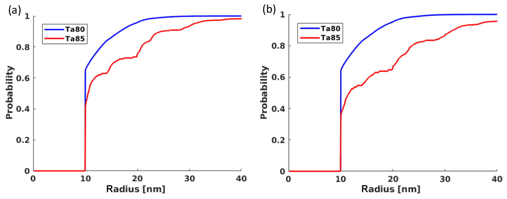
Figure 11Spherical contact distributions for the pore space in the xz slice at (a) 600 nm and (b) 1200 nm over the substrate. At these heights, Ta85 is clearly coarser than Ta80. Values less than 1 pixel are not considered – they are not reliable due to the fact that the data sets' resolution does not allow for structural details as small as pores to be differentiated.
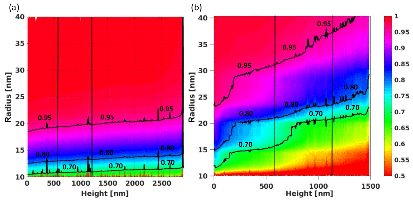
Figure 12Spherical contact distributions in xz slices as functions of the height over the substrate. Values of the spherical contact distributions given by the color map. The 70th, 80th, and 95th percentiles are delineated. Vertical lines at 600 and 1200 nm indicate the location of the curves represented in Fig. 11. Panel (a) represents Ta80, and panel (b) represents Ta85. For Ta80, the spherical contact distributions do not change significantly with height. The probability of reaching the solid within 20 nm of a random point in the pore space is nearly 1. For sample Ta85, this distance is considerably larger than in Ta80. Moreover, it clearly increases with height, which means that the comparably coarse pore structure becomes even coarser from bottom to top.
In our data, the pore space is only a few pixels thin which leads to overly rough estimated distributions when using conventional distance transform algorithms. Using a sub-pixel precision leads to better resolved distributions (Lindblad and Sladoje, 2015; Godehardt et al., 2019). Figure 11 shows the spherical contact distribution at 600 and 1200 nm for both samples. Analyzing the spherical contact distributions for all heights yields Fig. 12, where the colors denote the values of Hb(r). This, the spherical contact distribution again emphasizes that sample Ta85 is coarser than Ta80 and coarsens with increasing height. Namely, a deposition angle of 80∘ leads to structural similarity along the height, whereas a higher deposition angle of 85∘ leads to pore structure coarsening.
FIB-SEM imaging is a versatile method of obtaining images of porous materials at the nanoscale level that has the capacity to resolve nanostructures that cannot be detected with other conventional imaging methods.
Nevertheless, FIB-SEM images of porous material may have artifacts, which hamper the reconstruction of the structure. Thus, visual validation in every preprocessing step is critical to avoid errors during the process.
The mean porosity values from the 2-D images and the 3-D stack show good agreement. The evaluation of the 3-D stack and the high-resolution 2-D images reveals an average porosity that increases with the deposition angle. This is due to the fact that the distance between the nanostructures rises strongly with increasing deposition angle because the shadowing mechanism of the GLAD process intensifies the extinction of the nanostructures during film growth.
For a deposition angle of 80∘ (Ta80), average porosities of approximately 48 % (3-D stack) or 40 % (high-resolution 2-D image) result over the entire layer thickness. If the layer grows at a constant speed, a constant porosity profile across the layer thickness results at a fixed deposition rate on the quartz crystal monitor. The constant porosity profile at 80∘ confirms the assumption that the mobility of the incident particles is severely restricted by the substrate cooling.
For a deposition angle of 85∘ (Ta85), the results display average porosities of approximately 65 % (3-D stack) or 61 % (2-D image), with a slight increase in porosity from 60 % to 70 % across the layer thickness in the 3-D-stack. Again, the small increase in porosity demonstrates the influence of the substrate cooling.
The 3-D analysis based on the reconstructed structures is advantageous regarding analysis on highly resolved 2-D images because it determines spatial structural differences. Indeed, the structural analysis via the spherical contact function reports that the pore structure of sample Ta85 becomes coarser with rising height in comparison to sample Ta80.
Data are available upon request.
TO and SH designed and acquired the samples used in this study. DR, CR, KS, and MG performed the image processing, segmentation, and analysis of the reconstructed samples. TO, DR, KS, and SH wrote the paper with contributions from all authors. All authors contributed to the discussions.
The authors declare that they have no conflict of interest.
We acknowledge support from the Open Access Publication Funds of the SLUB/TU Dresden.
This research has been supported by the German Federal Ministry of Education and Research (grant no. 03VP00491/5), the German Academic Exchange Service (DAAD; Mathematics in Industry and Commerce Ph.D. program), and the German Research Foundation (grant no. GE 779/32).
This paper was edited by Ulrich Schmid and reviewed by two anonymous referees.
Albrecht, O., Zierold, R., Patzig, C., Bachmann, J., Sturm, C., Rheinländer, B., Grundmann, M., Görlitz, D., Rauschenbach, B., and Nielsch, K.: Tubular magnetic nanostructures based on glancing angle deposited templates and atomic layer deposition, Phys. Status Solidi, 247, 1365–1371, https://doi.org/10.1002/pssb.200945560, 2010. a
Alouach, H. and Fujiwara, H. M. G. J.: Magnetocrystalline anisotropy in glancing angle deposited Permalloy nanowire arrays, J. Vac. Sci. Technol. A, 23, 1046, https://doi.org/10.1116/1.1938978, 2005. a
Bassim, N., de Gregorio, B., Kilcoyne, A., Scott, K., Chou, T., Wirick, S., Cody, G., and Stroud, R.: Minimizing damage during FIB sample preparation of soft materials, J. Microsc., 245, 288–301, https://doi.org/10.1111/j.1365-2818.2011.03570.x, 2012. a
Beckers, N., Taschuk, M., and Brett, M.: Selective room temperature nanostructured thin film alcohol sensor as a virtual sensor array, Sensor. Actuat. B-Chem., 176, 1096–1102, https://doi.org/10.1016/j.snb.2012.09.041, 2013. a
Blevin, W. R. and Geist, J.: Influence of Black Coatings on Pyroelectric Detectors, Appl. Optics, 13, 1171, https://doi.org/10.1364/ao.13.001171, 1974. a
Bruggeman, D. A. G.: Berechnung verschiedener physikalischer Konstanten von heterogenen Substanzen. I. Dielektrizitätskonstanten und Leitfähigkeiten der Mischkörper aus isotropen Substanzen, Ann. Phys., 416, 636–664, https://doi.org/10.1002/andp.19354160705, 1935. a
Budzier, H. and Gerlach, G.: Thermal Infrared Sensors: Theory, Optimisation and Practice, John Wiley & Sons, https://doi.org/10.1002/9780470976913.ch6, 2011. a
Carl Zeiss Microscopy: ZEISS Atlas 5, available at: https://www.zeiss.de/mikroskopie/produkte/mikroskopsoftware/atlas.html#download, last access: 28 October 2019. a
Dice, G. D., Brett, M. J., Wang, D., and Buriak, J. M.: Fabrication and characterization of an electrically variable, nanospring based interferometer, Appl. Phys. Lett., 90, 253101, https://doi.org/10.1063/1.2749418, 2007. a
Fehrenbach, J., Weiss, P., and Lorenzo, C.: Variational Algorithms to Remove Stationary Noise: Applications to Microscopy Imaging, IEEE T. Image Process., 21, 4420–4430, 2012. a
Fitschen, J. H., Ma, J., and Schuff, S.: Removal of curtaining effects by a variational model with directional forward differences, Comput. Vis. Image Und., 155, 24–32, 2017. a, b, c
Garnett, J. C. M.: Colours in Metal Glasses and in Metallic Films, Philosophical Transactions of the Royal Society. Mathematical, Phys. Eng. Sci., 203, 385–420, https://doi.org/10.1098/rsta.1904.0024, 1904. a
Garnett, J. C. M.: Colours in Metal Glasses, in Metallic Films, and in Metallic Solutions. II, Philos. T. Roy. Soc., 205, 237–288, https://doi.org/10.1098/rsta.1906.0007, 1906. a
Godehardt, M., Mosbach, D., Roldan, D., and Schladitz, K.: Efficient 3D erosion dilation analysis by sub-pixel EDT, Mathematical Morphology and Its Applications to Signal and Image Processing, Proceedings 14th International Symposium, ISMM, Springer, 2019. a
Hawkeye, M. M. and Brett, M. J.: Glancing angle deposition: Fabrication, properties, and applications of micro- and nanostructured thin films, J. Vac. Sci. Technol. A, 25, 1317, https://doi.org/10.1116/1.2764082, 2007. a
Hawkeye, M. M., Taschuk, M. T., and Brett, M. J.: Glancing Angle Deposition of Thin Films, John Wiley & Sons, Ltd, https://doi.org/10.1002/9781118847510, 2014. a
Holzer, L., Stenzel, O., Pecho, O., Ott, T., Boiger, G., Gorbar, M., de Hazan, Y., Penner, D., Schneider, I., Cervera, R., and Gasser, P.: Fundamental relationships between 3D pore topology, electrolyte conduction and flow properties: Towards knowledge-based design of ceramic diaphragms for sensor applications, Materials and Design, 99, 314–327, https://doi.org/10.1016/j.matdes.2016.03.034, 2016. a
Hwang, S., Kwon, H., Chhajed, S., Byon, J. W., Baik, J. M., Im, J., Oh, S. H., Jang, H. W., Yoon, S. J., and Kim, J. K.: A near single crystalline TiO2nanohelix array: enhanced gas sensing performance and its application as a monolithically integrated electronic nose, The Analyst, 138, 443–450, https://doi.org/10.1039/c2an35932d, 2013. a
Joos, J., Carraro, T., Weber, A., and Ivers-Tiffée, E.: Reconstruction of porous electrodes by FIB/SEM for detailed microstructure modeling, J. Power Sources, 196, 7302–7307, https://doi.org/10.1016/j.jpowsour.2010.10.006, proceedings of 2010 European Solid Oxide Fuel Cell Forum, 2011. a
Kennedy, S. R., Brett, M. J., Toader, O., and John, S.: Fabrication of Tetragonal Square Spiral Photonic Crystals, Nano Lett., 2, 59–62, https://doi.org/10.1021/nl015635q, 2002. a
Kennedy, S. R., Brett, M. J., Miguez, H., Toader, O., and John, S.: Optical properties of a three-dimensional silicon square spiral photonic crystal, Photonic. Nanostruct., 1, 37–42, https://doi.org/10.1016/s1569-4410(03)00005-1, 2003. a
Krause, K., Vick, D., Malac, M., and Brett, M.: Taking a Little off the Top: Nanorod Array Morphology and Growth Studied by Focused Ion Beam Tomography, Langmuir, 26, 17558–17567, 2010. a
Krause, K., Thommes, M., and Brett, M. J.: Pore analysis of obliquely deposited nanostructures by krypton gas adsorption at 87K, Microporous and Mesoporous Materials, 143, 166–173, 2011. a
Lindblad, J. and Sladoje, N.: Exact Linear Time Euclidean Distance Transforms of Grid Line Sampled Shapes, in: Mathematical Morphology and Its Applications to Signal and Image Processing, edited by: Benediktsson, J. A., Chanussot, J., Najman, L., and Talbot, H., 645–656, Springer International Publishing, Cham, 2015. a
Liu, S., Sun, L., Gao, J., and Li, K.: A fast curtain-removal method for 3D FIB-SEM images of heterogeneous minerals, J. Microsc., 272, 3–11, 2018. a, b
Machado, E., M., N., Lathi, J., Schennach, R., Schmidt, V., and Zojer, K.: Pore space extraction and characterization of sack paper using μ-CT, J. Microsc., 272, 35–46, https://doi.org/10.1111/jmi.12730, 2018. a
Meijering, E., Niessen, W., and Viergever, M.: Quantitative Evaluation of Convolution-Based Methods for Medical Image Interpolation, Medical Image Analysis, 5, 111–126, 2001. a
Münch, B., Trtik, P., Marone, F., and Stampanoni, M.: Stripe and ring artifact removal with combined wavelet-Fourier filtering, Opt. Express, 17, 8567–8591, 2009. a, b
Ohser, J. and Mücklich, F.: Statistical Analysis of Microstructures in Materials Science, Wiley, Chichester, New York, 2000. a
Ohser, J. and Schladitz, K.: 3d Images of Materials Structures – Processing and Analysis, Wiley VCH, Weinheim, 2009. a, b
Penner, D. and Holzer, L.: Characterization and modelling of structure and transport properties of porous ceramics, Publikationen School of Engineering: ZHAW Digital Collection, 95, E27–E32, 2018. a
Prill, T., Schladitz, K., Jeulin, D., Faessel, M., and Wieser, C.: Morphological segmentation of FIB-SEM data of highly porous media, J. Microsc., 250, 77–87, 2013. a, b, c, d
Prill, T., Redenbach, C., Roldan, D., Godehardt, M., Schladitz, K., Höhn, S., and Sempf, K.: Simulating permeabilities based on 3D image data of a layered nano-porous membrane, Int. J. Solids Struct., in press, 2019. a, b, c
Robbie, K.: Advanced techniques for glancing angle deposition, J. Vac. Sci. Technol., 16, 1115, https://doi.org/10.1116/1.590019, 1998. a, b
Robbie, K., Friedrich, L. J., Dew, S. K., Smy, T., and Brett, M. J.: Fabrication of thin films with highly porous microstructures, J. Vac. Sci. Technol., 13, 1032–1035, https://doi.org/10.1116/1.579579, 1995. a
Salzer, M., Prill, T., Spettl, A., Jeulin, D., Schladitz, K., and Schmidt, V.: Quantitative comparison of segmentation algorithms for FIB-SEM images of porous media, J. Microsc., 257, 23–30, https://doi.org/10.1111/jmi.12182, 2015. a, b
Schankula, C., Anand, C., and D. Bassim, N.: Plasma Focused Ion Beam Curtaining Artifact Correction by Fourier-Based Linear Optimization Model, Microsc. Microanal., 24, 588–589, https://doi.org/10.1017/S1431927618003434, 2018. a
Schossig, M.: Ultradünne, freitragende Lithiumtantalat-Elemente für hochdetektive Infrarotsensoren, Dissertation, Fakultät für Elektrotechnik und Informationstechnik, TU Dresden, 2012a. a
Schossig, M.: Optical Absorption Layers for Infrared Radiation, in: Bio and Nano Packaging Techniques for Electron Devices: Advances in Electronic Device Packaging, edited by: Gerlach, G. and Wolter, K., chap. 18, 355–381, Springer Berlin Heidelberg, https://doi.org/10.1007/978-3-642-28522-6, 2012b. a
Schossig, M., Norkus, V., and Gerlach, G.: Infrared Responsivity of Pyroelectric Detectors With Nanostructured NiCr Thin-Film Absorber, IEEE Sensors Journal, 10, 1564–1565, https://doi.org/10.1109/JSEN.2010.2046162, 2010. a
Singh, J. P., Tang, F., Lu, T. K. T., and Wang, G.: Enhanced cold field emission from 〈100〉 oriented β-W nanoemitters, https://doi.org/10.1116/1.1736642, 2004. a
Soille, P.: Morphological Image Analysis, Springer, Berlin, Heidelberg, New York, 1999. a
Stenzel, O., Salzer, M., Schmidt, V., Cleary, P. W., and Delaney, G. W.: Quantitative structural analysis of simulated granular packings of non-spherical particles, Granular Matter, 16, 457–468, https://doi.org/10.1007/s10035-014-0486-4, 2014. a
Thevenaz, P., Ruttimann, U., and Unser, M.: A pyramid approach to subpixel registration based on intensity, IEEE T. Image Process., 7, 27–41, 1998. a
Tomus, D. and Pang, H.: In situ lift-out dedicated techniques using FIB-SEM system for TEM specimen preparation, Micron, 44, 115–119, https://doi.org/10.1016/j.micron.2012.05.006, 2013. a