the Creative Commons Attribution 4.0 License.
the Creative Commons Attribution 4.0 License.
 | 09 Oct 2019
A two-port electrothermal model for suspended MEMS device structures with multiple inputs
Monuko du Plessis
Advances in micromachining have led to the development of microelectromechanical systems (MEMS) devices with suspended structures used in a variety of sensors. Of note for this work are sensor types where two elements exist on the suspended membrane, including examples like air flow and differential pressure detectors, gas detection, and differential scanning calorimetry sensors. Intuitively one would argue that some thermal loss exists between the two elements. However, surprisingly little is documented about this electrothermal interaction. The work presented here addresses this shortcoming by defining a new parameter set, a matrix of thermal coupling coefficients. They are used within our novel two-port electrothermal model based on the heat flow equation adapted as a linear system of equations. However, the model is only effective with knowledge of these coefficients. We introduce an approach to extract the coefficients using finite-element method (FEM)-based multiphysics simulation tools and revisit and extend our previous method of non-ideal power coupling, this time to extract the coefficient matrix from measured data. Both specialist simulation tools and device manufacturing are very expensive. However, they are the only choices in the absence of an analytic model. A major contribution of this work is the derivation of a model to predict the coefficients by analytic means from the device dimensions and material properties. The research contribution and paper culminate in a comparison of analytic, simulated, and experimentally extracted values of two different devices to verify and demonstrate the effectiveness of the proposed models. The values compare well and show that the best results achieved are approximately 90 % and 70 % thermal linkage respectively for vacuum and atmospheric pressure conditions.


Electrothermal circuits (ETC) are circuits where the electrothermal interaction between components and the substrate is considered. Their analysis has been present in the literature since the early sixties (Matzen et al., 1964; Gray and Hamilton, 1971), but researchers have pursued it with less vigour than the purely electrical counterparts. This is mostly because of the large power consumption constraint associated with their operation (Louw et al., 1977). It was the commercialisation of MEMS manufacturing technologies that gave rise to a vast range of applications for ETC, notably because of the advances in micromachining. This led to high-yield, low-cost manufacturing and massive improvements in electrothermal performance. These applications have penetrated the industrial, military, and consumer markets, showing their diversity and the extensive marketing opportunities they present. Examples include the likes of on-chip sensors for diagnostics (Sisto et al., 2010; Zhang et al., 2009), chemical detection (Corsi et al., 2012; Barritault et al., 2013), thermal conductivity sensors (heat flow sensors and micro-hotplates) (Senesac et al., 2009; Arndt, 2002; Elmi et al., 2008), air flow sensors (Baltes et al., 1998; Johnson and Higashi, 1987; Simon et al., 2001), and thermal imaging microbolometers (Akula et al., 2011; Dulski et al., 2013; Castaldo et al., 1996; Liddiard, 2013).
The last two application areas are especially of interest in this work. Researchers have invested significant effort in improvements in the analytic modelling of the electrothermal effect, particularly for suspended membrane structures. Two recent introductions offer substantial improvements and are worth mentioning. First, joining a narrow and wide region results in an additional radial thermal conduction component. The restriction resistance model proposed is very effective and accounts for the additional component under vacuum conditions (Topaloglu et al., 2010). Second, an elliptical model better accounts for the radial temperature distribution on a suspended membrane in atmospheric pressure conditions (Schoeman and du Plessis, 2016). Both methods improve conventional models by up to 40 %.
Despite the continued active contributions in the modelling of traditional microbolometers, the detailed modelling of more generic dual-element devices, especially the interaction between these elements labelled as C in Fig. 1a, is lacking. This is surprising considering that these devices have existed for many years (Arndt, 2002; Yoon and Wise, 1994; Klaassen et al., 1995; Baltes et al., 1998). The approach in analytic electrothermal modelling of the detailed thermal interaction between the two devices or elements is never very rigorous and the interactions of the suspended elements with one another are mostly unclear. Authors typically assume perfect thermal linkage without mentioning the possibility of imperfect linkage. Furthermore, the electrical feedback network will often compensate for the imperfection. One technique offers an analytic solution to the temperature distribution of a thin-film resistor sensor pasted onto a large mass. However, the solutions are complex and time-consuming to solve. The author concludes that the model is useful for creating CAD tools (von Arx et al., 2000). This limits the practicality of the solutions.
It is interesting to note that the absence of an accurate analytical model for the electrothermal interaction can likely be attributed to the strength of the FEM simulation methodologies. However, these tools are very expensive and mostly used to simulate device-level behaviour, although some tools allow the capability of extracting the device model to a circuit-level model that can be used in SPICE-based simulation, but at an additional cost. As such, simpler SPICE models have been developed to couple the electrothermal parameters to electrical ones used in readout circuits for infrared microemitters and microbolometers (Kiran and Karunasiri, 1999; Nazdrowicz et al., 2015; Kim and Ko, 2015). However, we should highlight that the lack of an existing model hampers (i) the understanding and design of optimal thermal coupling devices and (ii) the design of effective readout circuits for ETC while accounting for thermal losses. This leaves a research gap that this paper will address. In Sect. 2 of this work we present a novel method to transform complex suspended device structures with two resistive elements into electrothermal equivalent microbeams that can be used to determine a matrix of thermal coupling coefficients. This is derived for both vacuum and atmospheric pressure conditions. We also propose that a multidimensional heat flow problem can be simplified and described using this set of coefficients within a linear system of equations modelling an equivalent electrothermal two-port system. Section 3 introduces a new simulation methodology to extract the matrix of coefficients. We also extend our experimental method introduced previously (Schoeman and du Plessis, 2012) for Ti1 at atmospheric pressure to account for the complete set of parameters required by the latest two-port model. In Sect. 4 we present and compare analytic, simulated, and experimental results for two different devices at two different pressure levels. Finally, we present some conclusions based on the results.
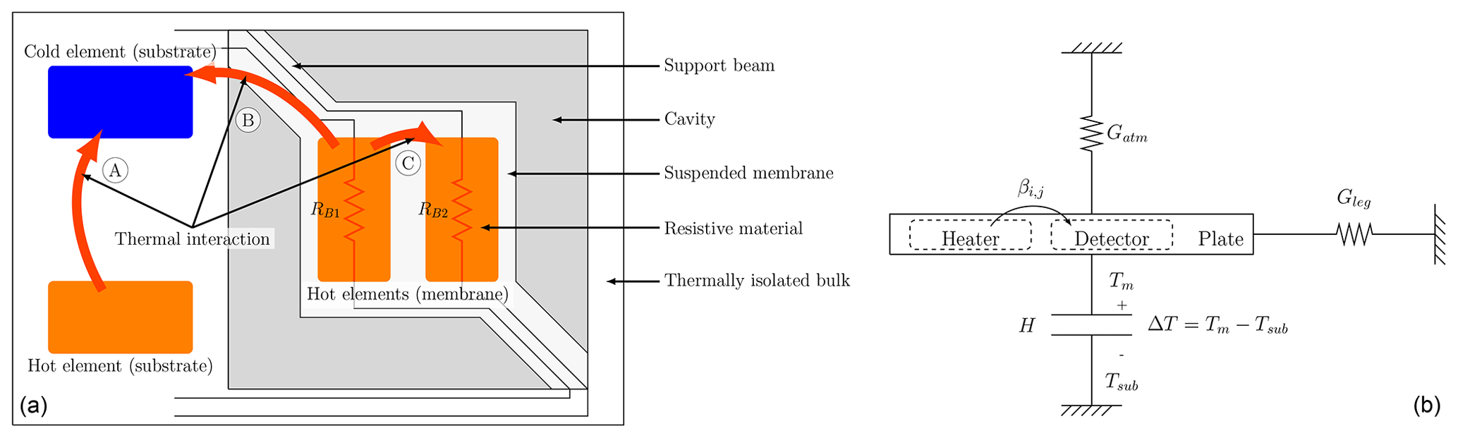
Figure 1The operating principles and the thermal model for a generic dual-resistive element device. (a) The device topology highlighting the required components of the device structure and the thermal linkage that exists between the resistive elements. (b) An equivalent heat flow diagram for a generic two-element device. The elements are labelled as the heater and detector, although each element can serve as both.
2.1 Operating principles of suspended devices
The device structure is similar to conventional microbolometers that are created by stacking multiple layers and removing a sacrificial layer by wet etching. The structure can be divided into two regions, (i) a membrane that is suspended over a cavity after etching and (ii) support beams to hold the membrane in position. This is illustrated in Fig. 1a. The suspended device has a thermal capacity that stores absorbed energy over time and acts as a heat reservoir. It can be heated by applying electrical power to a resistive material deposited on top of the suspended membrane. However, the resulting temperature gradient between the membrane and substrate will cause heat to flow from the warmer membrane to the cooler substrate through the support beams and the gas filling the cavity underneath the membrane. These thermal conductive components are referred to as the beam thermal conduction and the gaseous thermal conduction respectively. These interactions between the various components are illustrated in Fig. 1b and, with the exception of the thermal linkage components, are described by a heat flow model for conventional microbolometers blind to IR radiation stated mathematically as (Shie et al., 1996; Galeazzi and McCammon, 2003)
where H is the thermal capacity of the detector with unit J K−1, Gleg is the thermal conductance of the detector to the substrate via the supporting legs in W K−1 analogous to the thermal resistance that results in losses in heat, Gatm is the thermal conductance of the detector through the atmosphere to the substrate with unit W K−1, Tm is the temperature of the membrane in Kelvin, Tsub is the temperature of the substrate in Kelvin, Ta is the ambient temperature surrounding the membrane in Kelvin, and P is the electrical power applied to bias the resistive element in Watt. The equation is often simplified by assuming that (i) the substrate is at room temperature (Ta=Tsub) and/or (ii) the device operates at steady state (GeffΔT=P). An additional assumption is that Gatm=0 under vacuum conditions, simplifying Geff even further.
Geff consists of two components (Eriksson et al., 1997), one of which is a thermal conductance component attributed to heat loss between the suspended membrane and the substrate via the support beams referred to as the beam thermal conductance, Gleg. This is the dominant heat loss mechanism under vacuum conditions and is given by (Topaloglu et al., 2010; Niklaus et al., 2007)
with i an index to a specific layer, N the number of support beams (typically two or four), kb the effective thermal conductivity of the beam measured in W m−1 K−1, WB the width of the beam measured in metres, dth the thickness of the beam measured in metres, and LB the length of the beam measured in metres. Accounting for the radial thermal conductive component can significantly improve the estimation of the thermal conductivity. The transformed thermal conductivity is given by (Topaloglu et al., 2007)
where LM and WM are the membrane length and width respectively.
The second component contributing to Geff is the atmospheric or gaseous thermal conductance, Gatm. This is the dominant heat loss mechanism at atmospheric pressure and is given as (Niklaus et al., 2007)
where is the area of the membrane in metres squared used in conventional methods, kair is the thermal conductivity of air at room temperature and pressure (0.00284 W m−1 K−1), and dλ is the cavity depth measured in metres.
Up to this stage, we have only considered the modelling of a conventional microbolometer device. This is a device with two terminals and a single port where power can be applied. Therefore, thermal linkage does not exist. It would be natural to wonder what the impact on the heat flow equation would be when we introduce a second (or multiple) resistive element(s) to the suspended device. This would allow for an additional port to the device through which we can control the plate temperature. The steady-state equivalent of Eq. (1) can be changed to allow for the perspective from the kth input as
where Pk is the biasing electrical power of the kth detector element in Watt and Tm,k is the average temperature increase of the membrane in Kelvin resulting from the applied power component Pk. Furthermore, we should be able to observe a portion of the power applied to one port on every other port of the device, since the resistive elements all share the same thermal reservoir. This suggests that the elements are thermally linked to each other, and we introduce a parameter, βi,j, to describe this thermal linkage. Since each resistive element will contribute towards a portion of the total change in the average membrane temperature, we propose to model the effective or total thermal increase as a system of linear equations, best described in vector form as
where is the average temperature increase of the membrane consisting of incremental temperature increases resulting from the biasing of the respective resistive elements, P is a power vector consisting of the power applied to each individual resistor, and is the matrix of weighted directional thermal coupling coefficients that exist between the various resistive elements. Here it is assumed that Geff is a constant scalar value for the developed structure which holds true for symmetric designs.
Therefore, the heat balance equation for a dual-element device in the steady state can be given by
from which we can easily solve the respective individual element average temperature increases if is known. The latter is relatively simple to determine from simulation and experimentally, as shown in Sect. 3. However, the analytic approach proves more challenging, as elaborated on next.
2.2 An analytic solution for the thermal coupling coefficients
Researchers have published comprehensive techniques for modelling the electrothermal behaviour of device structures with various degrees of similarity to our own. Examples include temperature profiling by solving the general heat flow partial differential equation (PDE) first developed and solved by Fourier, reducing dimensionality for specific applications by transformation, applying lumped thermal element analysis, and considering thermal coupling in the context of Seeback and Peltier effects. As expected, the intent is often to find one or more mechanical properties. We use similar methods that culminate in a robust approximate model to describe the electrothermal effect. The novel model consists of three parts: (i) finding the thermal coupling coefficients for two points on a microbeam, (ii) transforming between the microbeam and a more complex structure, and (iii) increasing the number of points by averaging over the entire resistive length. Each part is elaborated on next in a separate subsection.
2.2.1 Determine the coupling coefficient between two points on a microbeam
A number of examples exist where the steady-state heat transfer, well known to be governed by a second-order PDE, is solved analytically to find the temperature profile of a microbeam, cantilever, or similar rectangular MEMS type structures, which is then in turn further developed to solve some mechanical property, be it displacement, deflection, dampening, stresses, or elasticity (Chow and Lai, 2009; Kokkas, 1974; Huang and Lee, 1999; Yan et al., 2004; Mankame and Ananthasuresh, 2001). We use a similar approach to derive an expression for the newly proposed thermal coupling coefficients.
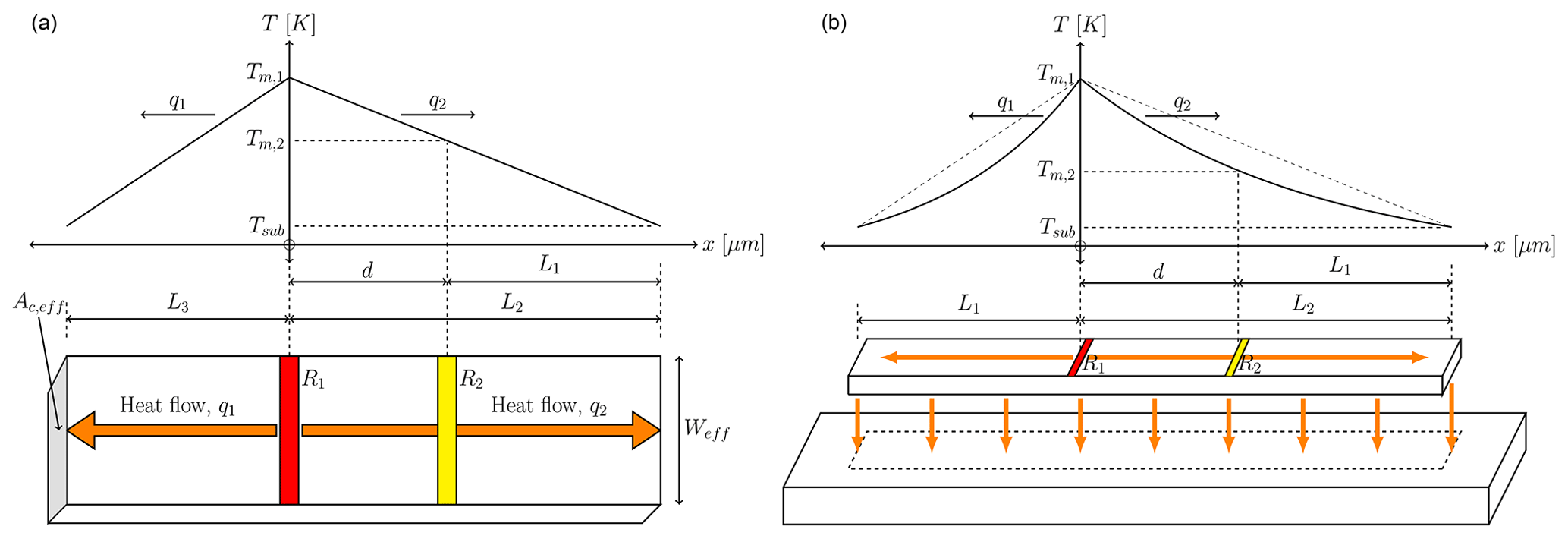
Figure 2A microbeam with two resistive strips and the relevant dimensions, along with the expected temperature profiles over the length of the bar. (a) The temperature profile through a microbeam when heat flow occurs only through the microbeam is typical under vacuum conditions. (b) The temperature profile through a microbeam when heat flow occurs through both the solid components of the microbeam, as well as the medium (either a gas or a fluid) between the microbeam and a heat sink.
First, consider a microbeam with two resistive components as illustrated in Fig. 2a. R1 is heated to a specific temperature Tm,1 that results in two heat flow vectors. One of these, q2, flows through R2 that experiences an increase in temperature in response. We know that under vacuum conditions the simplest form of a second-order linear homogeneous differential equation describes heat diffusion, given by . The differential equation is solved by double integration and a particular solution is found from the general solution. The former is given by
We define a new parameter, the thermal coupling coefficient β2,1, as a ratio of temperature differences. Substitution of the parameters in Fig. 2a into Eq. (8) yields
The problem is more complex when the device operates at atmospheric pressure since an additional gaseous thermal conduction component exists. This is illustrated in Fig. 2b. The best approach to derive a solution is to model the problem as a distributed thermal resistance network with rs and gair the unit components for the solid thermal resistance and the gaseous thermal conduction respectively. The temperature distribution is found by solving the standard form of a second-order linear homogeneous differential equation if the system is in steady state. This is given by
with K=rsgair. The roots of the quadratic equation may be solved and, after defining boundary conditions, the particular solution can be shown to be given by
It is insightful to consider the parameter Lch, the characteristic thermal length governing the exponential decay observed for the temperature over distance, given by
for a multilayered device structure and approximately 10 µm for our devices. The thermal coupling coefficient follows from the definition earlier in Eq. (9) and is given by
It should be clear that the coupling coefficient depends on the ratio of the separation distance between the resistive elements and the characteristic length of the microbeam in an exponential manner. The thermal coupling can be maximised by reducing the separation distance of the resistive elements in a design.
2.2.2 Transform between microbeams and suspended plate structures
It is also desirable to calculate thermal linkage for more complex device geometries. This should be possible if the more complex geometry can be transformed into a simpler microbeam and the thermal coupling coefficients of the previous section is applied. In general, transformations between device geometries are not new and examples include multidimensional structure transformation into cylindrical coordinates (Khan and Falconi, 2013; Sberveglieri and Hellmich, 1997; Simon et al., 2001). Our approach is quite different and is based on an equivalent heat flow vector analysis.
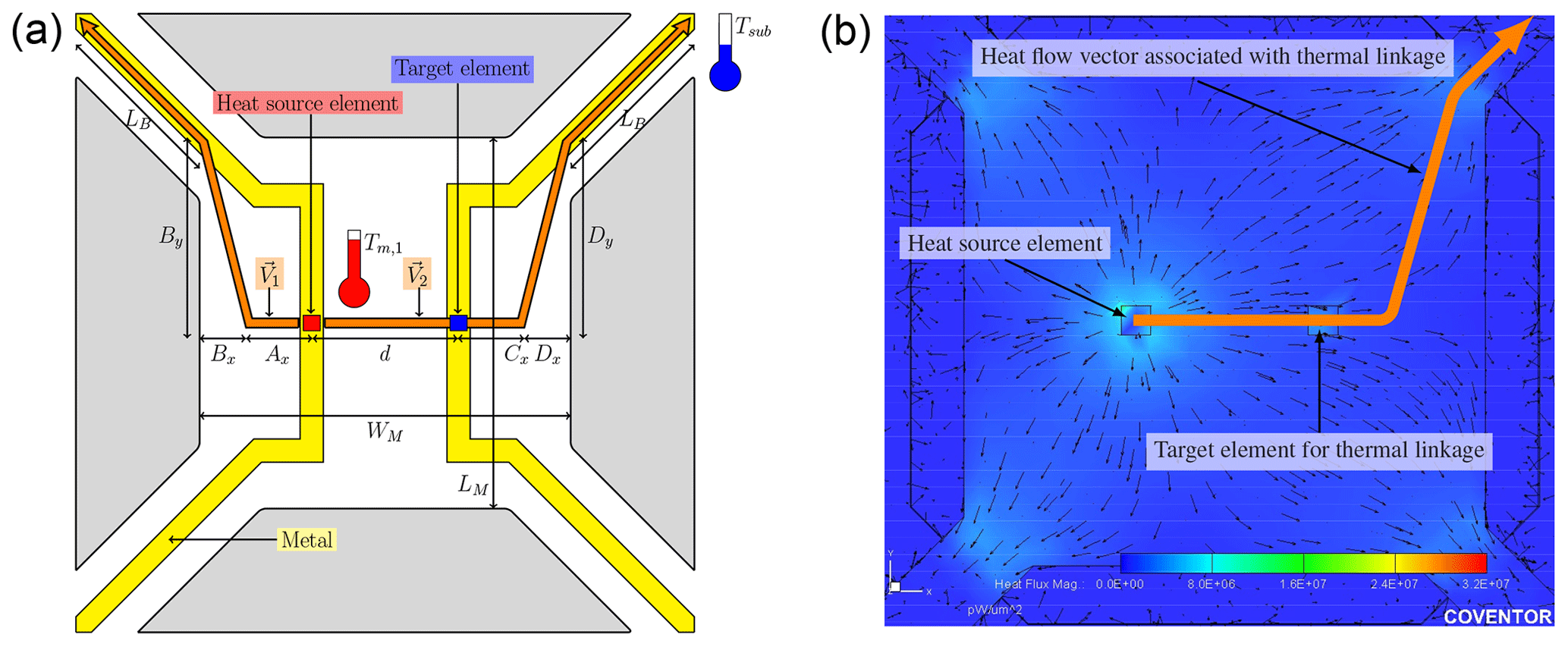
Figure 3A graphical illustration of the heat flow vector of interest that results in thermal linkage for a dual-element suspended plate with four support beams. A simulation model with a simplified elemental heat source supports the proposal. (a) A structural overview of the device with the relevant dimensions indicated. The proposed vectors are indicated by the orange arrows, while a single heat source element is indicated as a red square and the target element on the opposing resistor is indicated by a blue square. (b) A simulation result showing the heat flow vectors from a single source element as well as the proposed heat flow vector (indicated by the orange arrow) resulting in the thermal linkage between the heat source and target.
We propose that the equivalent heat flow of interest from a specific heat source point through a specific target element will occur only along a single vector as illustrated in Fig. 3b. This should be intuitive, but can also be observed from the supporting FEM simulation result of Fig. 3b. The simulation result also shows an infinite amount of additional heat flow vectors, but recall that the desired solution is the single vector flowing through the target element. Therefore, we only need to consider the vector V2.
Closer inspection reveals that V2 extends from the heat source towards the closest point on the second resistive element where thermal linkage occurs, after which the vector extends by some fraction Cm past R2. It changes direction towards the connection between the support beam and the membrane and finally extends along the support beam towards the substrate. V2 is stated mathematically as
and the distance between the heat source point and the substrate is calculated by
where Cm is a proportionality constant (a typical value is 0.5) that describes the depth of penetration of C in the x direction before V2 changes direction, WM is the width of the membrane, LB is the length of the support beam, and d is the separation distance between the source and target points. It should become immediately clear after inspection of Eq. (15) that this vector is in the form . This can be used to relate a suspended plate structure, like a microbolometer, to the microbeam of the previous section and allows for the calculation of L1, a microbeam parameter, as a function of the plate dimensions.
A complete transformation between the two structures is possible if the effective thermal resistance experienced by V2 is the same as that of the equivalent microbeam. This occurs if the microbeam has an effective width given by
where and Δx2=LB.
2.2.3 Determine an average coupling coefficient over the entire resistor length
The model components developed thus far for thermal linkage between two single points are not very useful until the concepts are extended to apply to heaters and detectors with more practical lengths. As such, we introduce the notion of dividing the heater and detector elements into unique regions and applying an averaging mechanism. To classify a region as unique, we identify the parts of the heater that have a constant separation distance to the detector. Every such length with a unique separation distance would make up a unique region. A number of k such regions can exist for a device, but the thermal linkage is optimised by reducing the number of regions, with k=1 being optimal. We illustrate the concept of regions in Fig. 4 and show examples in Sect. 2.3. We can use the entire length of a region as part of the weighting coefficient, .
Furthermore, a length of the heater element might be associated with more than one region. This increases computational complexity, but when considering Eqs. (9) and (13) we realise that the increase in separation distance dramatically reduces the thermal linkage. We can simplify the problem and find an approximate solution by only considering the region with the smallest separation distance for any length of the heater. Therefore, a region only needs to be coupled to its closest neighbouring region on the alternate resistor, with the remaining regions considered insignificant. These considerations result in an averaging algorithm given by
with jn being the single nearest neighbour only of the particular ith region. This results in a computational reduction, often to the extent that the thermal coupling can be computed quickly by hand without the need for simulation. An example is provided at the end of the next section.
2.3 Device designs
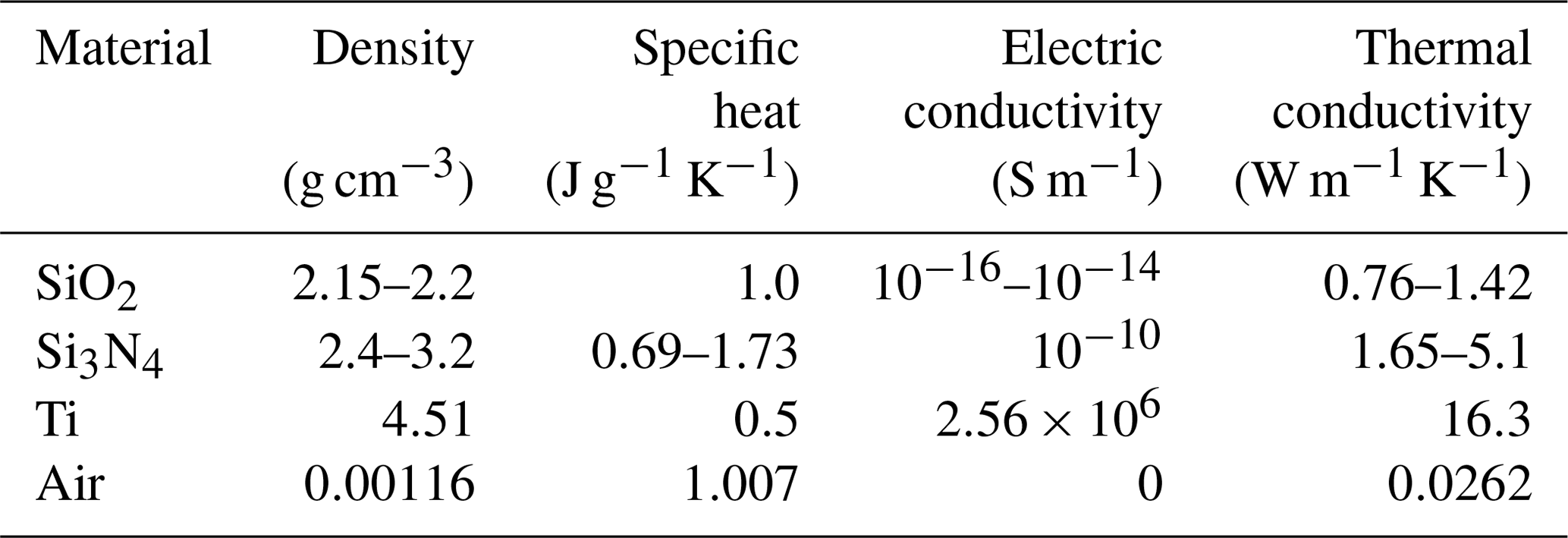
The material properties of the materials used to construct the suspended devices play a significant role in the device performance parameters. Notably, the thermal conductivity, ki, of the materials used to construct the support beams plays a role in the thermal conductance, Gleg, especially that of silicon nitride in typical suspended plate designs. The various material densities, ρi, and specific heat, ci, play a major role in the thermal time response, τ, and the thermal capacity, H, of the devices. The relevant properties are summarised in Table 1.
Table 1A summary of the most important material properties that are used in the manufacturing of the test devices.
The manufactured Ti thin-film dual resistive element devices are shown in Fig. 4 with the dimensions relevant to Eq. (17) superimposed on the images. Earlier, the plate dimensions were defined and shown in Fig. 3a. Take note of the additional parameters: (i) the length of the first Ti thin-film resistor, LR,1, (ii) the width of the first resistor, WR,1, and (iii) the length of the coupling region between the resistive elements, di,j. The length and the width of the second Ti thin-film resistor are not indicated, but they are defined in the same way as for the first resistor. A summary of the device designs and their dimensions and surface characteristics are provided in Table 2, while the linkage parameters are compared in Table 3.
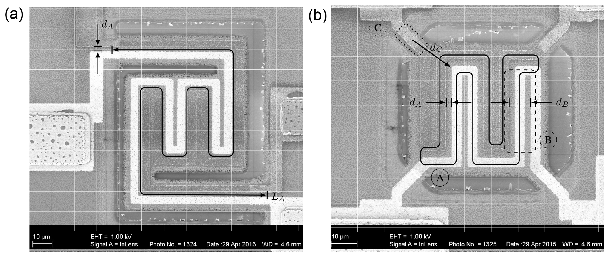
Figure 4SEM micrographs of the various manufactured test structures with the relevant thermal linkage parameters indicated. Regions are identified and defined as parts of the design that have a constant separation distance di over the entire resistance length of that region. (a) A suspended plate structure (Ti1) with optimal thermal linkage. (b) A suspended plate structure (Ti2) with high thermal linkage.
Table 2A summary of the Ti thin-film dual-element device dimensions.
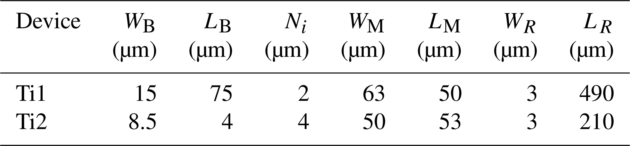
Table 3A summary of the device parameters required by the proposed analytic model to determine the thermal linkage.
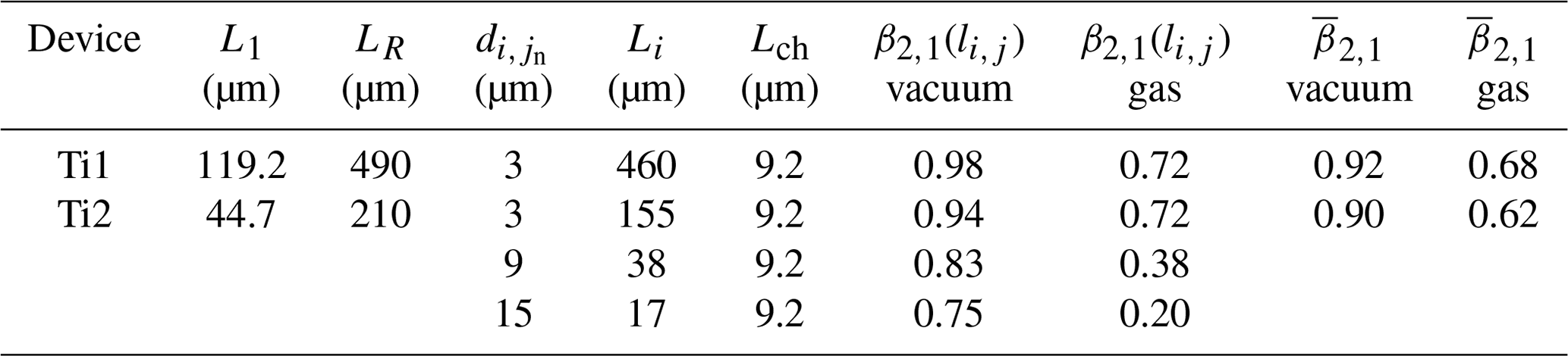
A device (Ti1) optimised for a very high thermal coupling coefficient is illustrated in Fig. 4a. The device features two Ti thin-film resistors with a separation distance dA=3 µm over the entire length of the resistors µm. A second device, Ti2, offers a high thermal coupling coefficient and is illustrated in Fig. 4b with the device dimensions specified in Table 2. The device has a resistance length µm and is divided into three unique regions (A, B, and C) with region lengths LA=155, LB=38, and LC=8.5 µm and separation distances dA=3, dB=9, and dC=15 µm.
3.1 Approach followed in the simulation study
Multiphysics simulation platforms are highly effective in simulating 3-D device structures. We opted to use Coventorware, an industry leading multiphysics MEMS simulator, for the study. The standard material properties database of the simulation software is used and the values correspond closely to those in Table 1. A thermomechanical solver is selected to simulate thermoelectric physics in the steady state by applying an electrical potential to the gold contacts of the device as a boundary condition and then to investigate the resulting thermal effects. The substrate is considered a thermal heat sink with constant temperature, which can be applied as a fixed boundary condition where the substrate temperature is selected as 300 K. During the steady-state analysis, the input potentials of both resistors are swept independently over their respective voltage ranges and the resulting average temperature changes of the resistive elements are noted.
The parameters of the heat balance equation of Eq. (6) are solved in two parts. First, recall that each value in the coupling coefficient matrix, , is in the form of the proposed definition of Eq. (9). These coefficients are solved by applying a controlled average temperature stimulus to only one element and then extracting the average element temperature increase of the alternate element to find the ratios as
Secondly, once is known, the effective thermal conductance is solved from Eq. (7) when rewritten as
where for symmetric device designs.
3.2 Approach followed for the experimental method
The experimental method requires three parts to solve the parameters of the heat balance equation of Eq. (6). First, we use a popular purely electrical method that is widely used in industry for microbolometers to solve the temperature coefficient of resistance (TCR), α, in a controlled oven with variable temperature (Shie et al., 1996). Second, the device voltage is measured when sweeping the input current using a parameter analyser. The device resistance can then be calculated from the measured results. In turn, Geff may be extracted by finding the slope of the inverse resistance as a function of the square of the biasing current that is given by
as a linear equation with the different ports of the device.
The third and final step is to notice from Eq. (7) that the average temperature increase of one element can be solved by applying a controlled power stimulus to the alternate resistive element while ensuring that no power is applied to the element under investigation, from which the set of equations reduces to provide the thermal coupling coefficients as
which is equivalent to
This implies that the resistance of the first element can be increased by a value equivalent to compared to the reference resistance. The modulation of the resistance RB1 is controlled by P2 and the effect is illustrated in Fig. 5. The figure also serves to further clarify the differences in the contributions of Tm,1 (or P1) and Tm,2 (or P2). Although not indicated in the figure, the same modulation concept will hold true for the resistance of the second element, , by applying a control signal to the first element.

Figure 5Effect on the resistance in terms of the current stimuli. The bottom graph represents the reference curve when biasing the first resistive element alone, while the top graph shows the additional increased resistance when the second resistor is also biased.
The analytically predicted results of the devices are provided in Table 3. However, to verify the validity of the theoretical model and reach a meaningful conclusion, those results need to be compared to results of simulation and experimental methods that extract the coupling coefficients. As such, the simulation and experimental results obtained for the two thermally coupled MEMS devices are presented next for both vacuum and atmospheric pressure conditions.
Table 4A comparison of the thermal beam conductance of the Ti thin-film dual-element devices under vacuum conditions.
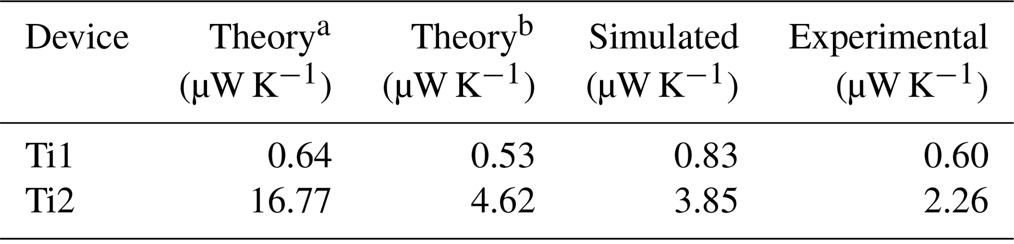
Table 5A comparison of the total thermal conductance of the devices at atmospheric pressure.

Table 6A comparison of the average thermal coupling coefficient, , of the devices under vacuum conditions.

Table 7A comparison of the average thermal coupling coefficient, , of the dual-element devices at atmospheric pressure.
4.1 Simulation results of the thin-film metal devices
The first results presented are of a simulated parametric voltage sweep applied to the gold contacts of RB1, ranging from 0 to 0.25 V, while RB2 remains unbiased. This offers a benchmark result similar to what is measured for conventional microbolometers. Once the benchmark curve is obtained, the potential applied across RB2 is increased in 0.05 V increments up to 0.25 V. These increments are indicated with labels A through E in Fig. 6. At each increment, the original potential sweep applied to RB1 is repeated. The average temperatures of the thin-film Ti resistors are extracted at each point of the multivariable sweep, with the results for the first element plotted in Fig. 6c. These results are also used to extract the electrical power dissipated by the device. These are combined as the P–T curve illustrated in Fig. 6d that serves to extract the beam thermal conductances from the slopes. Note that these are intermediate results. Therefore, only the results of Ti1 under vacuum conditions are presented for brevity. The same method is followed for atmospheric pressure conditions and repeated for device Ti2 under both conditions.
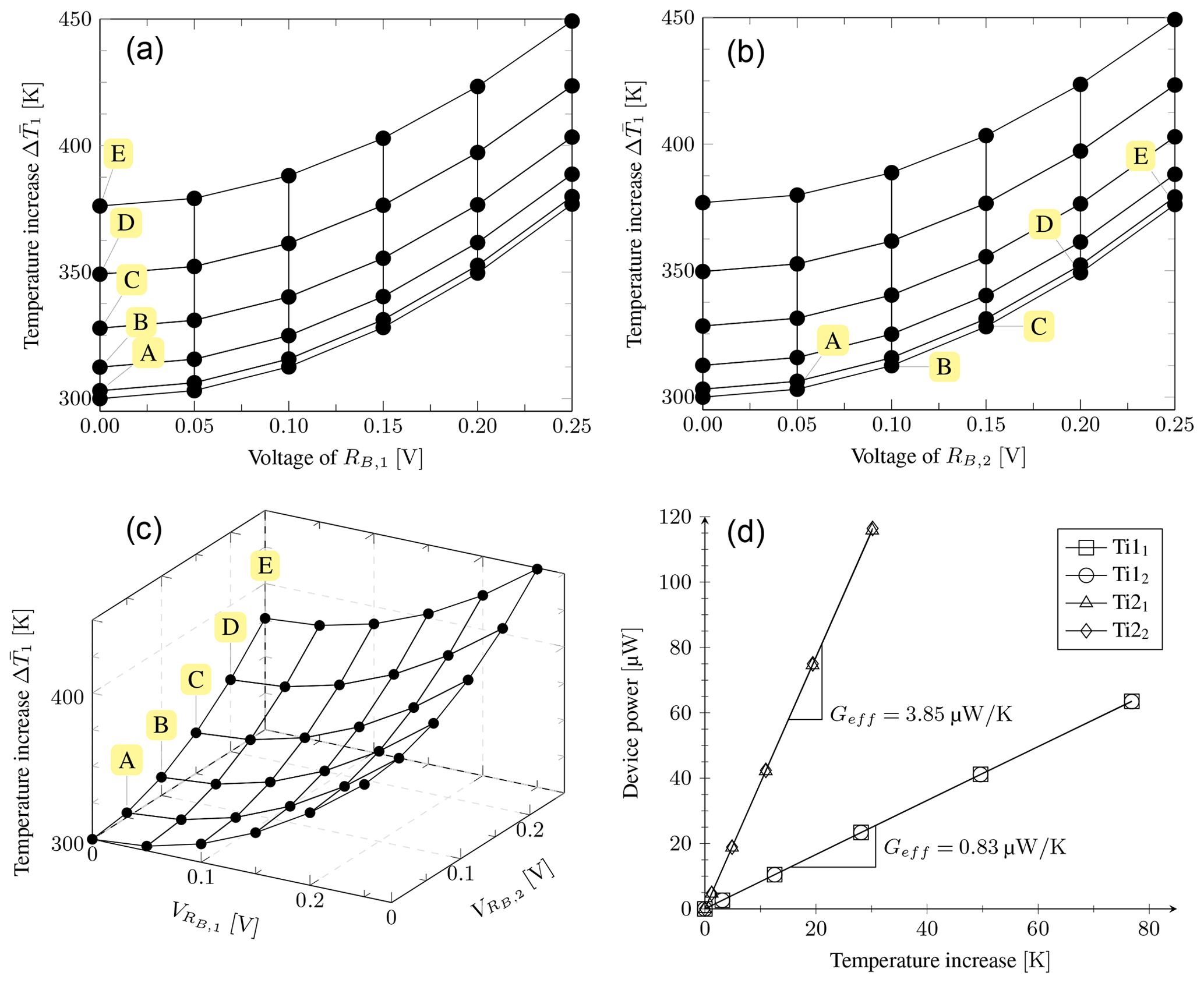
Figure 6Simulation results of the thermoelectric interaction that exists for the Ti devices under vacuum conditions. (a) XZ projection of the thermal profile of RB1 for Ti1. (b) YZ projection of the thermal profile of RB1 for Ti1. (c) 3-D thermal profile of RB1 for Ti1. (d) Temperature curves at different power levels to extract the beam thermal conductance.
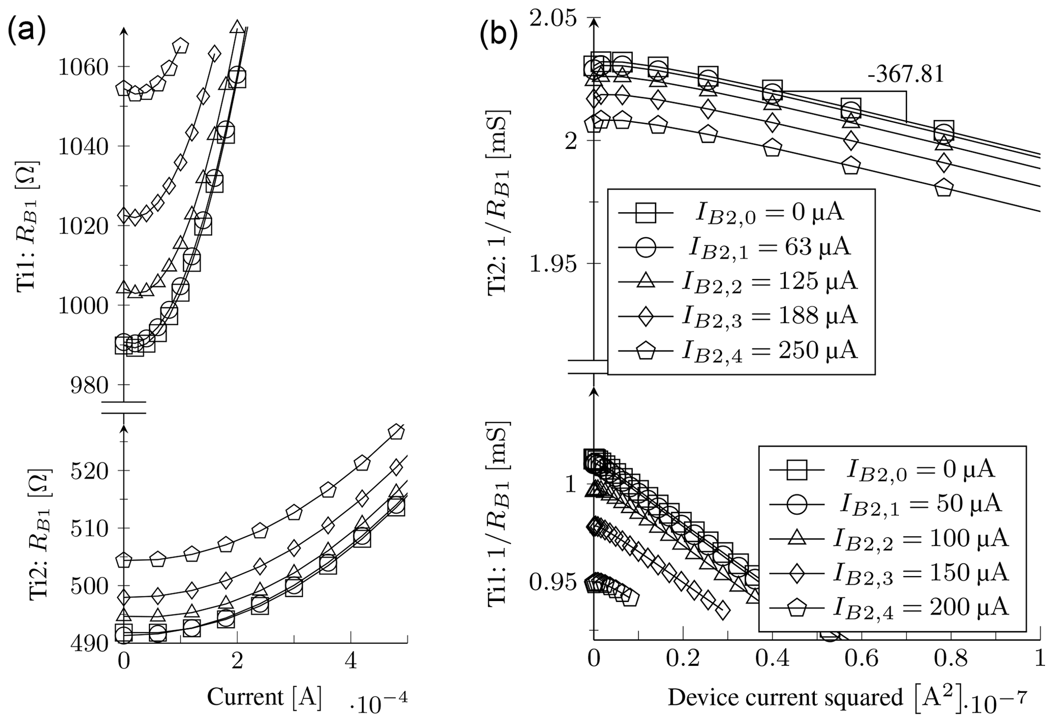
Figure 7Experimental results of a parametric current sweep under vacuum conditions for the Ti thin-film devices indicating the resulting resistance of the first resistive element, RB1, while RB2 is biased at different values as indicated in the legend entries. These results are also used to extract the beam thermal conductance. Note that the legends of (b) also apply to (a) but that Ti1 is presented at the top of (a) and at the bottom of (b), as expected when comparing R to 1∕R. (a) Experimental R–I curves. (b) Experimental 1∕R–I2 curves.
4.2 Measurement results of the thin-film metal devices
The V–I curves are useful to calculate the power dissipation of the devices, since Geff is extracted from this. The R–I curves also provide additional graphical insight into the resistive modulation effect. The next results show the experimental measurements of both devices in Fig. 7a. The sensed element voltage is measured when applying an input current sweep under vacuum conditions with the Hewlett Packard 4155B parameter analyser. The input current IB1 is swept up to 500 µA for the devices within the evacuated dewar as long as a maximum power consumption limit of 100 µW is met. The lower curves serve as the reference since µA. Once the reference curves have been obtained, the experiment is repeated at increments of approximately µA and µA respectively for devices Ti1 and Ti2. A very high thermal increase is possible even at moderate power consumption levels for Ti1 because of the low beam thermal conductance. This explains the need to limit the power consumption of the experiment. The slope of the curves suggests a positive TCR as expected for metal devices. The 1∕R–I2 curves are also indicated and used to extract the effective thermal conductance using Eq. (20). The results are plotted in Fig. 7b.
4.3 Comparison and discussion of the results
A comparison of the effective thermal conductances for the devices is provided in Table 4. The theoretically derived values using both Eqs. (2) and (3) are compared to the simulation results extracted from Fig. 6d and the experimental results extracted from Fig. 7b. The results compare very well overall, but the experimentally obtained value for Ti2 is slightly smaller than anticipated. This is due to mask alignment difficulties encountered during manufacturing, as seen in the SEM micrograph in Fig. 4b. This led to the left support beams playing a smaller role in the thermal isolation of the membrane than expected. We do notice a large discrepancy between the analytic and simulated results for device Ti2 at atmospheric pressure conditions. This warranted a deeper investigation into the particular design. It revealed that the entire plate of the simulated device does not reach the average temperature of the heater, which means Aeff is much smaller than the value used in the prediction. This leads to a smaller simulated thermal conductance. This is similar to an effect we first observed in conventional microbolometer designs (Schoeman and du Plessis, 2016). Also notice that the experimental values are smaller than those simulated. The simulation is set up with dλ=2 µm. However, microscopic inspection revealed that the devices are bending upwards. This was confirmed by a profilometric analysis, and it was found that Ti1 is bending upwards with dλ in excess of 3 µm and Ti2, with its shorter supports, measuring dλ=2.8 µm. This reduces the thermal conductance considerably, as expected from Eq. (4).
We use the methods of Sect. 3.1 and Sect. 3.2 to determine the thermal linkage between the resistive elements. Three biasing points, [0, 20, 100] % of the maximum IB1, are selected on each of the IB2,2–4 curves plotted in Fig. 7a. This results in nine data points for each device. We can use each result to extract a thermal coupling coefficient with Eq. (22) at that biasing point. The nine results are then averaged. The analytic, simulation, and experimental results obtained under vacuum conditions are presented in Table 6, while the same results at atmospheric pressure are presented in Table 7. As can be seen from the tabulated average thermal coupling coefficients, the predicted results of the Ti thin-film devices compare very well with the simulation and experimental results. The largest observed errors relative to the developed model are 7.6 % and 16.1 % respectively for the simulation and experimental results.
In this work, an analytic method is presented to quantify the thermal linkage expected between two resistive elements that share the suspended membrane of a MEMS device. This is a crucial component currently lacking in the complete modelling of the electrothermal interaction of such devices. We have confidence in the intermediate results, since the simulated and experimentally obtained thermal conductance values achieved are reasonable and compare well with what has been reported in the literature for conventional microbolometers. These devices compare well with our suspended structures. However, our thermal conductance values are larger within reason since our beam widths are increased to allow for the additional electrical connections of the second resistor. We have demonstrated, with both simulation and experimental measurement using manufactured devices, that the proposed model adequately predicts the thermal coupling effect. The main reason for the success of the model lies in the definition of Eq. (17). The best results are achieved and performance is optimised for coupling over very long lengths of resistors while maintaining a very small separation distance between them. This is typically achieved with long and narrow resistors, or LR≫WR, and hence, thin-film resistive materials are very suitable. Ti-based devices, for example, are ideal and outperform alternative material choices like VOx from our experience. We conclude that the developed model offers a reasonable output that will prove very useful in future MEMS designs of applications making use of thermal coupling. Other than the applications mentioned in the introduction, this effect holds potential in the low-frequency domain for solutions of MEMS-based on-chip electrothermal isolators and even signal processing. Designers using alternative design simulation methods, for example at a circuit level using SPICE to simulate ETC, also stand to benefit from the proposed analytic model, since it allows for a simple method to calculate the thermal linkage between elements without the need to use expensive device-level FEM software. This will be the focus of future work. Even our best thermal linkage results of approximately 90 % and 70 %, depending on the pressure conditions, are far from 100 %. As such, designers should be cautious to assume ideal thermal linkage, which is often assumed in previous work, and consider incorporating thermal coupling coefficients into their ETC designs.
The underlying simulation and measurement data are not publicly available and can be requested from the authors if required.
MdP initiated the work by acquiring funding that facilitated the necessary resources and software for design, simulation, and prototyping, offered invaluable insight during discussions, and supervised the work. JS developed the theoretical models, implemented the simulation models, developed and conducted the experimental work, carried out data processing and analysis, and drafted the manuscript.
The authors declare that they have no conflict of interest.
The authors thank the Advanced Manufacturing Technology Strategy (AMTS) of the Department of Science and Technology, South Africa, for the financial support of the research, as well as the National Research Foundation (NRF) for the Sabbatical Grants to Complete Doctoral Degrees Funding Instrument (UID number 86451).
This paper was edited by Michael Kraft and reviewed by two anonymous referees.
Akula, A., Ghosh, R., Sardana, H., Predeep, P., Thakur, M., and Varma, M. R.: Thermal Imaging And Its Application In Defence Systems, in: AIP Conference Proceedings-American Institute of Physics, 1391, p. 333, 2011. a
Arndt, M.: Micromachined thermal conductivity hydrogen detector for automotive applications, in: Proceedings of IEEE Sensors, 2, 1571–1575, https://doi.org/10.1109/ICSENS.2002.1037357, 2002. a, b
Baltes, H., Paul, O., and Brand, O.: Micromachined thermally based CMOS microsensors, P. IEEE, 86, 1660–1678, https://doi.org/10.1109/5.704271, 1998. a, b
Barritault, P., Brun, M., Lartigue, O., Willemin, J., Ouvrier-Buffet, J.-L., Pocas, S., and Nicoletti, S.: Low power CO2 NDIR sensing using a micro-bolometer detector and a micro-hotplate IR-source, Sensor. Actuat. B, 182, 565–570, https://doi.org/10.1016/j.snb.2013.03.048, 2013. a
Castaldo, R., Franck, C. C., and Smith, A. B.: Evaluation of FLIR/IR camera technology for airport surface surveillance, in: Enhanced and Synthetic Vision, 2736, 64–74, https://doi.org/10.1117/12.241047, 1996. a
Chow, J. and Lai, Y.: Displacement sensing of a micro-electro-thermal actuator using a monolithically integrated thermal sensor, Sensor. Actuat. A, 150, 137–143, https://doi.org/10.1016/j.sna.2008.11.014, 2009. a
Corsi, C., Dundee, A., Laurenzi, P., Liberatore, N., Luciani, D., Mengali, S., Mercuri, A., Pifferi, A., Simeoni, Mirko Tosone, G., Viola, R., and Zintu, D.: Chemical Warfare Agents Analyzer Based on Low Cost, Room Temperature, and Infrared Microbolometer Smart Sensors, Advances in Optical Technologies, 808541, https://doi.org/10.1155/2012/808541, 2012. a
Dulski, R., Bareła, J., Trzaskawka, P., and Pia̧tkowski, T.: Application of infrared uncooled cameras in surveillance systems, in: Electro-Optical and Infrared Systems: Technology and Applications X, 8896, 315–322, https://doi.org/10.1117/12.2028507, 2013. a
Elmi, I., Zampolli, S., Cozzani, E., Mancarella, F., and Cardinali, G.: Development of ultra-low-power consumption {MOX} sensors with ppb-level VOC detection capabilities for emerging applications, Sensor. Actuat. B, 135, 342–351, https://doi.org/10.1016/j.snb.2008.09.002, 2008. a
Eriksson, P., Andersson, J., and Stemme, G.: Thermal characterization of surface-micromachined silicon nitride membranes for thermal infrared detectors, J. Microelectromech. S., 6, 55–61, https://doi.org/10.1109/84.557531, 1997. a
Galeazzi, M. and McCammon, D.: Microcalorimeter and bolometer model, J. of Appl. Phys., 93, 4856–4869, 2003. a
Gray, P. R. and Hamilton, D. J.: Analysis of Electrothermal Integrated Circuits, IEEE J.Solid-St. Circ., 6, 8–14, https://doi.org/10.1109/JSSC.1971.1050152, 1971. a
Huang, Q.-A. and Lee, N. K. S.: Analysis and design of polysilicon thermal flexure actuator, J. Micromech. Microeng., 9, 64–70, https://doi.org/10.1088/0960-1317/9/1/308, 1999. a
Johnson, R. and Higashi, R.: A highly sensitive silicon chip microtransducer for air flow and differential pressure sensing applications, Sensor. Actuat., 11, 63–72, https://doi.org/10.1016/0250-6874(87)85005-9, 1987. a
Khan, U. and Falconi, C.: Temperature distribution in membrane-type micro-hot-plates with circular geometry, Sensor. Actuat. B, 177, 535–542, 2013. a
Kim, G. and Ko, H.: Behavioral modeling and experimental validation of uncooled microbolometer, in: 2015 IEEE SENSORS, 1–3, https://doi.org/10.1109/ICSENS.2015.7370392, 2015. a
Kiran, S. and Karunasiri, G.: Electro-thermal modelling of infrared microemitters using PSPICE, Sensor. Actuat. A, 72, 110–114, https://doi.org/10.1016/S0924-4247(98)00215-5, 1999. a
Klaassen, E. H., Reay, R. J., and Kovacs, G. T. A.: Diode-based Thermal RMS Converter With On-chip Circuitry Fabricated Using Standard CMOS Technology, in: Solid-State Sensors and Actuators, 1995 and Eurosensors IX. Transducers '95. The 8th International Conference on, 1, 154–157, https://doi.org/10.1109/SENSOR.1995.717119, 1995. a
Kokkas, A. G.: Thermal analysis of multiple-layer structures, IEEE T. Electron Dev., 21, 674–681, https://doi.org/10.1109/T-ED.1974.17993, 1974. a
Liddiard, K. C.: Application of mosaic pixel microbolometer technology to very high-performance, low-cost thermography and pedestrian detection, in: Infrared Technology and Applications XXXIX, 8704, 8704, 980–988, https://doi.org/10.1117/12.2018593, 2013. a
Louw, W. J., Hamilton, D. J., and Kerwin, W. J.: Inductor-less, capacitor-less state-variable electrothermal filters, IEEE J. Solid-St. Circ., 12, 416–424, https://doi.org/10.1109/JSSC.1977.1050923, 1977. a
Mankame, N. D. and Ananthasuresh, G. K.: Comprehensive thermal modelling and characterization of an electro-thermal-compliant microactuator, J. Micromech. Microeng., 11, 452–462, https://doi.org/10.1088/0960-1317/11/5/303, 2001. a
Matzen, W. T., Meadows, R. A., Merryman, J. D., and Emmons, S. P.: Thermal techniques as applied to functional electronic blocks, P. IEEE, 52, 1496–1501, https://doi.org/10.1109/PROC.1964.3438, 1964. a
Nazdrowicz, J., Szermer, M., Maj, C., Zabierowski, W., and Napieralski, A.: A study on microbolometer electro-thermal circuit modelling, in: 2015 22nd International Conference Mixed Design of Integrated Circuits Systems (MIXDES), 458–463, https://doi.org/10.1109/MIXDES.2015.7208563, 2015. a
Niklaus, F., Jansson, C., Decharat, A., Källhammer, J.-E., Pettersson, H., and Stemme, G.: Uncooled infrared bolometer arrays operating in a low to medium vacuum atmosphere: performance model and tradeoffs, in: Defense and Security Symposium, International Society for Optics and Photonics, 65421M–65421M, 2007. a, b
Sberveglieri, G., Hellmich, W., and Müller, G.: Silicon hotplates for metal oxide gas sensor elements, Microsyst. Technol., 3, 183–190, https://doi.org/10.1007/s005420050078, 1997. a
Schoeman, J. and du Plessis, M.: Characterisation of the Electrical Response of a Novel Dual Element Thermistor for Low Frequency Applications, SAIEE Africa Research Journal, 103, 9–13, https://doi.org/10.23919/SAIEE.2012.8531972, 2012. a
Schoeman, J. and du Plessis, M.: An analytic model employing an elliptical surface area to determine the gaseous thermal conductance of uncooled VOx microbolometers, Sensor. Actuat. A, 250, 229–236, https://doi.org/10.1016/j.sna.2016.09.033, 2016. a, b
Senesac, L. R., Yi, D., Greve, A., Hales, J. H., Davis, Z. J., Nicholson, D. M., Boisen, A., and Thundat, T.: Micro-differential thermal analysis detection of adsorbed explosive molecules using microfabricated bridges, Rev. Sci. Instrum., 80, 035102, https://doi.org/10.1063/1.3090881, 2009. a
Shie, J.-S., Chen, Y.-M., Ou-Yang, M., and Chou, B. C. S.: Characterization and Modeling of Metal-Film Microbolometer, Journal of Mircoelectromechanical Systems, 5, 298–306, 1996. a, b
Simon, I., Bârsan, N., Bauer, M., and Weimar, U.: Micromachined metal oxide gas sensors: opportunities to improve sensor performance, Sensor. Actuat. B, 73, 1–26, https://doi.org/10.1016/S0925-4005(00)00639-0, 2001. a, b
Sisto, M. M., Garcia-Blanco, S., Le Noc, L., Tremblay, B., Desroches, Y., Caron, J.-S., Provencal, F., and Picard, F.: Pressure sensing in vacuum hermetic micropackaging for MOEMS-MEMS, J. Micro-Nanolith., MEM., 9, 041109–041109, 2010. a
Topaloglu, N., Nieva, P., Yavuz, M., and Huissoon, J.: A Novel Method for Estimating the Thermal Conductance of Uncooled Microbolometer Pixels, in: IEEE International Symposium on Industrial Electronics, ISIE 2007, 1554–1558, https://doi.org/10.1109/ISIE.2007.4374834, 2007. a
Topaloglu, N., Nieva, P. M., Yavuz, M., and Huissoon, J. P.: Modeling of thermal conductance in an uncooled microbolometer pixel, Sensor. Actuat. A, 157, 235–245, https://doi.org/10.1016/j.sna.2009.11.018, 2010. a, b
von Arx, M., Paul, O., and Baltes, H.: Process-dependent thin-film thermal conductivities for thermal CMOS MEMS, J. Microelectromech. S., 9, 136–145, https://doi.org/10.1109/84.825788, 2000. a
Yan, D., Khajepour, A., and Mansour, R.: Design and modeling of a MEMS bidirectional vertical thermal actuator, J. Micromech. Microeng., 14, 841–850, https://doi.org/10.1088/0960-1317/14/7/002, 2004. a
Yoon, E. and Wise, K. D.: A wideband monolithic RMS-DC converter using micromachined diaphragm structures, IEEE T. Electron Dev., 41, 1666–1668, https://doi.org/10.1109/16.310122, 1994. a
Zhang, J., Jiang, W., Zhou, J., and Wang, X.: A simple micro Pirani vacuum gauge fabricated by bulk micromachining technology, in: Solid-State Sensors, Actuators and Microsystems Conference, 2009. TRANSDUCERS 2009. International, 280–283, https://doi.org/10.1109/SENSOR.2009.5285508, 2009. a