the Creative Commons Attribution 4.0 License.
the Creative Commons Attribution 4.0 License.
 | 09 Jan 2018
Granular metal–carbon nanocomposites as piezoresistive sensor films – Part 1: Experimental results and morphology
Günter Schultes
Hanna Schmid-Engel
Silvan Schwebke
Ulf Werner
We have produced granular films based on carbon and different transition metals by means of plasma deposition processes. Some of the films possess an increased strain sensitivity compared to metallic films. They respond to strain almost linearly with gauge factors of up to 30 if strained longitudinally, while in the transverse direction about half of the effect is still measured. In addition, the film's thermal coefficient of resistance is adjustable by the metal concentration. The influence of metal concentration was investigated for the elements Ni, Pd, Fe, Pt, W, and Cr, while the elements Co, Au, Ag, Al, Ti, and Cu were studied briefly. Only Ni and Pd have a pronounced strain sensitivity at 55 ± 5 at. % (atomic percent) of metal, among which Ni–C is far more stable. Two phases are identified by transmission electron microscopy and X-ray diffraction: metal-containing nanocolumns densely packed in a surrounding carbon phase. We differentiate three groups of metals, due to their respective affinity to carbon. It turns out that only nickel has the capability to bond and form a stable and closed encapsulation of GLC around each nanoparticle. In this structure, the electron transport is in part accomplished by tunneling processes across the basal planes of the graphitic encapsulation. Hence, we hold these tunneling processes responsible for the increased gauge factors of Ni–C composites. The other elements are unable to form graphitic encapsulations and thus do not exhibit elevated gauge factors.
- Article
(8122 KB) - Full-text XML
- Companion paper
- BibTeX
- EndNote


Inorganic carbon-based thin films attract a lot of attention, not only in solid-state research but also in different application fields. The subgroup of transition-metal–carbon films (Me–C) is, of its own right, a large research field with thousands of papers published in the last three decades since the original work by Dimigen et al. (1987). A review of sputter-deposited transition-metal carbides and the nanocomposite's microscopic structures was published by Jansson and Lewin (2013). Such films are beneficial in many applications ranging from tribological hard coatings to magnetics, sensing, and energy conversion. Metal–carbon films are heterogeneous because they form nanocomposites with either amorphous or crystalline regions inside a matrix of carbon. Transition metals in contact with carbon behave very differently due to their distinct affinity to carbon. Precious metals like Cu, Au, and Pt are completely immiscible; they form isolated crystalline nanoparticles inside the carbon matrix. On the contrary, metals such as Cr, Ti, and W have a strong affinity to carbon and form thermodynamically stable and hard metallic carbides. In between are metals like Ni, Co, and Fe with a low affinity to carbon. These metals are still able to interact with carbon but the reaction products depend on many parameters like, for example, the deposition technique, substrate temperature, and metal content (Bayer et al., 2016). For instance, nickel is a prominent catalyst in the production of carbon nanotubes and graphene (Garlow et al., 2016).
Our research is focused on metal–carbon thin films as sensor layers for strain and related quantities such as pressure, force, and torque. An elevated piezoresistivity was described for nickel-containing hydrogenated amorphous carbon Ni:a–C:H in 2006 (Schultes et al., 2006), while more physical and structural properties were published subsequently (Koppert et al., 2009, 2012; Heckmann et al., 2011; Petersen et al., 2011, 2012). In the present paper, we expand the investigations to 12 different transition metals in carbon (Me–C), explore their sensing properties, and aim to understand the reason for elevated strain sensitivity in terms of microscopic morphology.
We deployed two different plasma deposition techniques for the generation of metal–carbon thin films in this work. Although the majority of depositions are based on a combined reactive PVD/CVD plasma process, some other sets of samples were produced by means of a PVD co-sputter process. We briefly characterize the most important features of the two processes.
Reactively deposited films of Me:a–C:H are obtained when adding the precursor ethylene (C2H4, 99.95 % purity) into argon gas (40 sccm (standard cubic centimeters per minute), 99.999 % purity) while sputtering from a metal target. This combined PVD/CVD process (RF-diode without magnetron) carried out on a MRC model 822 is described in more detail elsewhere (Koppert et al., 2012). Prior to deposition, the substrates were cleaned and pre-heated in the load lock for 30 min to 300 ∘C. The sputtering process was conducted at a pressure of 2.8 Pa with varying C2H4 ∕ Ar ratios of 0.625 to 6.75 % to produce films of different composition. A metal target (diameter 125 mm, distance to substrate 60 mm) driven by RF-power (13.56 MHz) yields a controlled target self-bias voltage of −1700 V. Simultaneously, a substrate RF-power of −100 V was added to foster the energy intake onto the samples placed on the static carrier plate. Adapted deposition times between 0.5 and 40 min are necessary for film thicknesses in the range of 20 to 1050 nm. Directly after deposition, the sample carrier was transferred into the load lock for a post annealing at 300 ∘C for 30 min (unless otherwise specified) without breaking the vacuum. Both heating processes as well as bias-assisted sputtering are necessary to fully cultivate the desired high gauge factors of the sensor layers.
A different PVD tool was deployed for the non-reactive processes generating hydrogen-free Me:a–C layers. This tool is homebuild and equipped with separate magnetron targets of carbon (graphite) and metal (diameter 52 mm, distance 120 mm) driven by adjustable DC-power supplies. An effective substrate heating with halogen lamps underneath the rotating substrate carrier is realized; however, no substrate bias is feasible. Argon with a flow of 30 sccm and a pressure between 0.8 and 2 Pa is led into the chamber. A plasma driving DC-power of 200 W is applied on the graphite target while varying the power of 8 to 37 W on the metal target to obtain different concentrations.
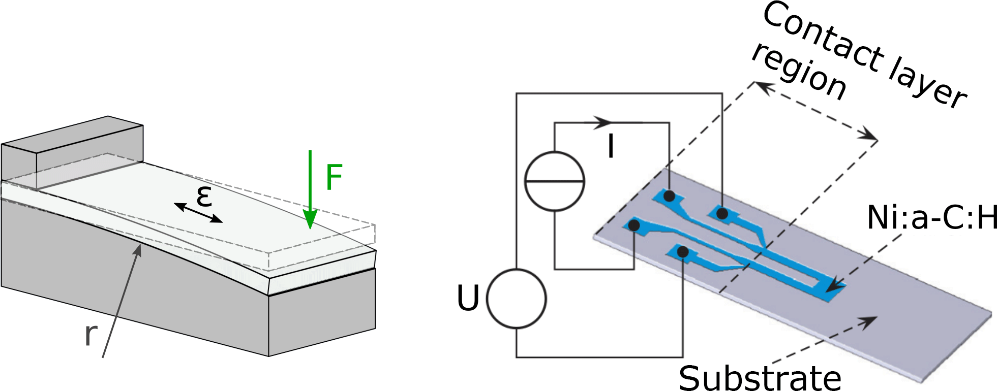
Figure 1Scheme of the bending device. The force F bends the sample into a curve of radius r inducing a strain ε. A sample with a U-shaped structure of the Me–C film, and four contacts for the gauge factor and the temperature coefficient of resistivity (TCR) determination, are shown.
For the intended investigations, films were deposited mainly on two kinds of substrates: Al2O3 (Rubalit® 710 Alumina, by CeramTec) and Si/SiO2 including an oxide layer (800 nm thick) to provide an appropriate insulation. Rubalit® is quite rough with an arithmetic average value of the surface roughness Ra of 75 nm, in contrast to Si/SiO2 having a smooth surface with Ra of only 0.5 nm. Both substrate types have a thickness of 0.38 mm with dimensions of 12 mm × 30 mm. To obtain measurable structures we used simple shadow masks of stainless steel or a lift-off process with aluminum negative structures described elsewhere (Koppert et al., 2012). The resistance has the shape of a U (with dimensions of the legs of 5 mm × 1 mm) comprising of 12.5 squares with strongly varying resistance values due to different thicknesses and respective concentrations of metal and carbon. With these types of brittle substrates, we measure the strain-induced resistance change at a small and given level of strain ε with the bending device of Fig. 1. The strain can be expressed by the bending radius r and the thickness d of the substrate.
The sample is deformed by bending on a curved metallic block with a radius of 840 mm inducing a strain ε of 2.3 × 10⁻⁴ (0.023 %) along the longitudinal sample direction. Samples are clamped at one end by an insulating PEEK-block (polyether ether ketone) holding four pins that contact the film for a four-point measurement of the electrical resistance (Fig. 1) using an Agilent 34970A multimeter. The multimeter is mostly operated in the 10 kΩ range with 100 µA current and thus working in the range of 1 V excitation voltage. We assume the strain perpendicular to the depicted direction to be negligibly small, as verified by finite element analysis. The gauge factor (k) is obtained from the electrical resistances of the film structure in both states: unloaded at rest (R0) and if bent (Rε) onto the radius according to the following equation:
We used the U-shaped structure because it represents a common layout for strain measurements. However, it consists of two paths parallel to strain (i.e., longitudinal, kL) and a short path perpendicular to strain (i.e., transverse, kT). Due to different lengths, the transverse paths only contribute at most 20 % of the longitudinal one. Hence, the gauge factor k is a value between kT and kL, close to the latter. For a separate determination of kT and kL, we designed different structures that are introduced in Sect. 3.3.
When put into an oven, this setup is also very useful to measure the temperature effects on the gauge factor and the temperature coefficient of resistivity (TCR) due to temperature changes from T0 = 30 ∘C to T1 = 55 ∘C of the unstrained resistances.
However, this bending method of brittle substrates is not adequate for different and higher strain values. Therefore, we also prepared thin films on a flexible and stretchable polymer foil. For this purpose, a measurement structure was deposited onto polyimide foil (DuPont) having a thickness of 50 µm. The foil is then elongated in a tensile test by means of a testing machine (Zwick), recording the resistance change versus strain in a wider range of ε from 0 to 2 × 10⁻² (2 %). Under these circumstances, we have to consider a transverse contraction of the foil due to its Poisson ratio of 0.34.
The elemental compositions of the Me–C thin films were determined by energy dispersive X-ray (EDX) spectroscopy in a scanning electron microscope (JEOL 6460LV) equipped with an Oxford Inka 300 spectrometer. For this purpose, we deposited films on single crystalline silicon substrates. The structure was characterized by grazing incidence X-ray diffraction (GIXRD) with CuKα radiation (λ = 0.15406 nm) on a Bruker D8 Focus X-ray diffractometer. To study the microstructure of the thin films and the lattice structure, transmission electron microscopy (TEM) studies were conducted using a Philips CM 200 FEG. We prepared top-view TEM specimens as films with thicknesses of around 50–70 nm on Si3N4 membranes (purchased from Plano) whereas cross-section samples were cut with a focused ion beam system.
We will first present the mechano-electrical measurements of nickel–carbon films, i.e., the strain sensitivity on different substrates, the gauge factors and TCRs over a broad range of film thickness, and the distinction of longitudinal and transversal gauge factors. Then we will extend the investigation to other metal–carbon films including 12 different transition metals and reveal the extraordinary role of nickel–carbon. At last, our morphology studies are presented, elucidating the reason for enhanced sensitivity.
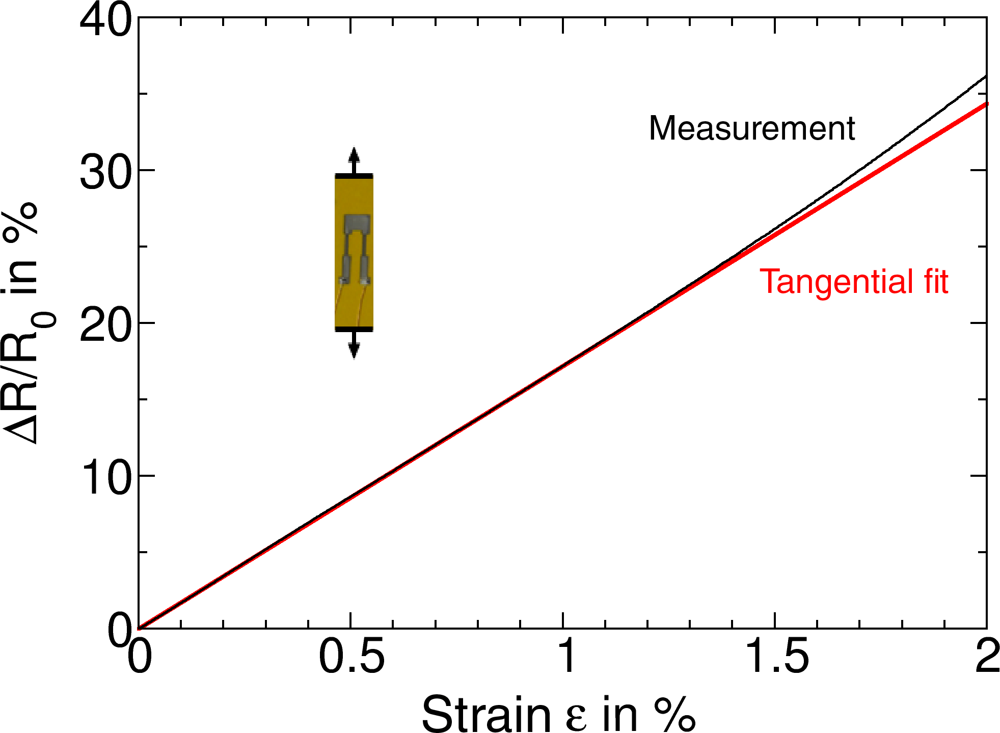
Figure 2The measured resistance change of a Ni:a–C:H film on polyimide foil due to tensile strain. A linear fit is added to the measurement.
3.1 Strain sensitivity versus strain
We start by discussing films of Ni:a–C:H (55 ± 5 at. % Ni, 150 nm thickness) on polyimide foil exposed to increasing strain from 0 to 2 % in a tensile test. The foil carried a structured resistance (approx. 5 kΩ) comprising two legs as depicted in Fig. 2. The testing machine slowly strained the sample during 20 min to 2 % of strain while measuring the resistance.
A typical result of one of many samples reveals a nearly linear dependence of the resistance with a gauge factor k = 17 over the displayed strain range (Fig. 2). Thus, the gauge factor is nearly independent of the strain level. At even higher strain levels, starting at 3 %, more important deviations from linearity occur that are attributed to the beginning of a plastic deformation of the polyimide foil and a partly irreversible resistance change. The nearly linear dependence is very distinct from reports on functionalized Au-cluster films (Herrmann et al., 2007) and on Pt:Al2O3 cermet films (Puyoo et al., 2017) that obviously show exponential behavior.
The resistance change would be even higher without the influence of a transverse contraction that we have to face in this setup. The elongation εL provokes a perpendicular contraction of εT = −εL ⋅ μ with Poisson ratio μ = 0.34 (of polyimide). εT in turn will diminish the resistance change with its transversal sensitivity (kT). Thus, we have the following:
As we will show later in this paper kT ≈ 0.5 ⋅ kL.
Therefore, the longitudinal gauge factor would be kL ≈ 20.5 in this experiment, as would be measured under sole longitudinal strain.
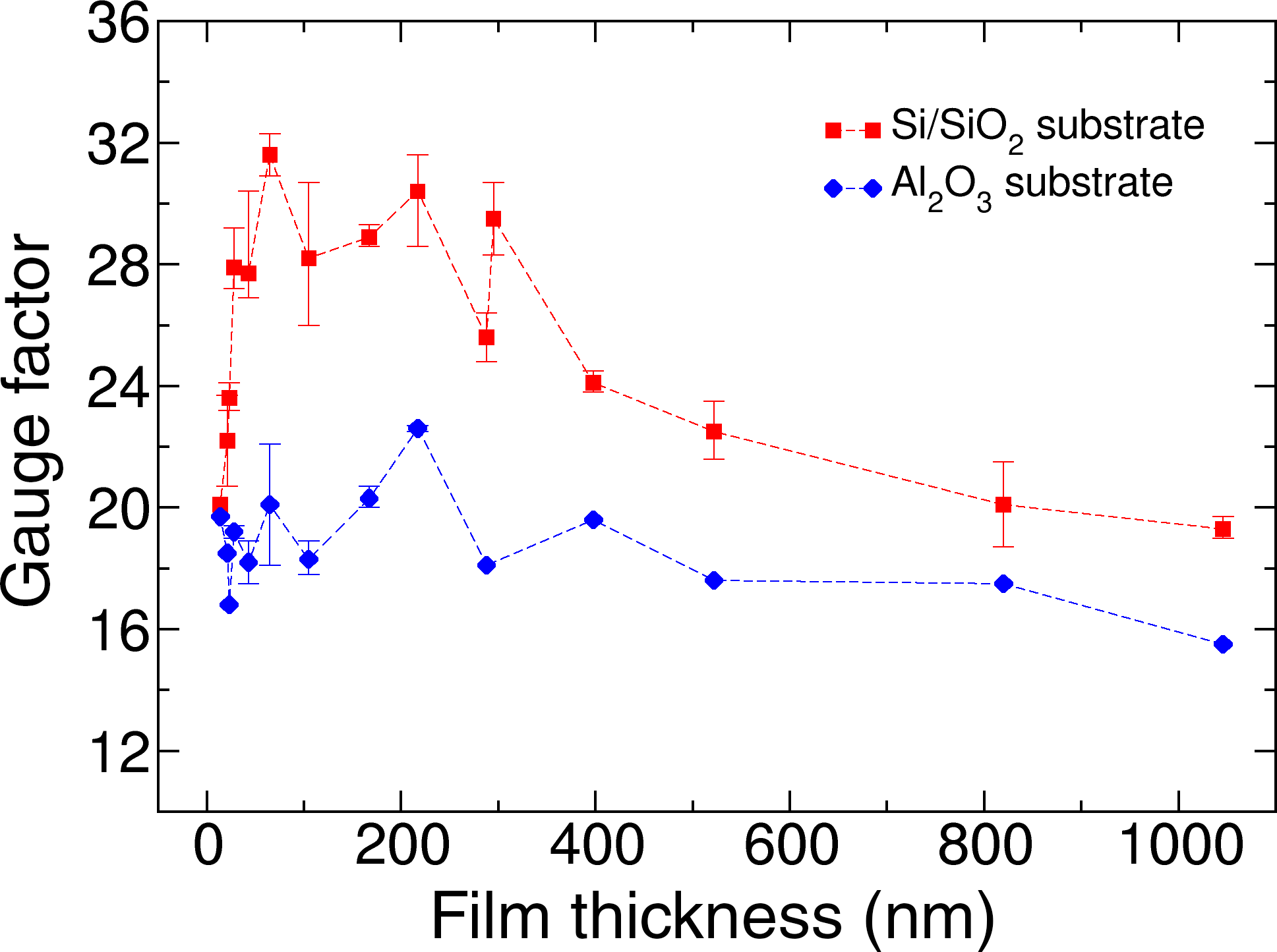
Figure 3Gauge factors of Ni:a–C:H with 55 ± 5 at. % Ni films versus film thickness. Red dots represent measurements on substrates of Si∕SiO2, with a very smooth surface. Gauge factors on substrates of Al2O3 – plotted in blue dots – are generally lower, which is mainly attributed to a higher roughness of the substrates. The lines are added to guide the eye.
3.2 Gauge factors and TCR versus film thickness on different surfaces
Next we studied the role of film thicknesses and the influences of different substrate surfaces on the gauge factor. Si/SiO2 with a smooth surface (Ra 0.5 nm) and rough alumina plates (Ra 75 nm) served as substrates. As the sensitivity is nearly independent of strain, as demonstrated in Fig. 2, we used the bending setup described above exerting only a low level of strain (ε = 0.023 %). Samples with 55 ± 5 at. % Ni were deposited through shadow masks with always the same pre- and post heat treatment by adjusting the deposition time from 30 s to 40 min. This resulted in a large range of film thicknesses from 20 to 1050 nm. The sheet resistance varies according to the film thickness, but the gauge factor does not correlate in an easy way with the thickness as shown in Fig. 3.
The type of substrate influences the gauge factor. The highest values are measured on the smooth Si wafers. Even semi-transparent films with thicknesses less than 20 nm are still highly sensitive. Figure 3 reveals several findings: films of some 60 to 250 nm of thickness have the highest sensitivities with significantly higher values for the smoother surface of Si/SiO2. The gauge factors of 30 ± 2 are the highest values in metal–carbon systems we have measured so far. Regarding a rough surface with hills and valleys (on alumina) the applied strain ε of the sample results in lower local strains on the slopes and thus reduces the gauge factors. With increasing film thickness, the surface roughness becomes less important, hence, the sensitivities on both substrates approach each other. In addition, the sensitivity decreases for higher thicknesses. For a possible explanation, we have to consider the morphology of the films. As we will show in our microscopic analysis later in this paper, we are faced with columns of Ni or Ni3C encapsulated by walls of graphite-like carbon (GLC). The columns are not perfectly aligned and not perfectly separated from each other by carbon walls. Instead, we observe some links and contacts over the length of the columns. With increasing thickness, the columns thus become more connected, raising the contribution of metallic conduction and thereby reducing the gauge factor.
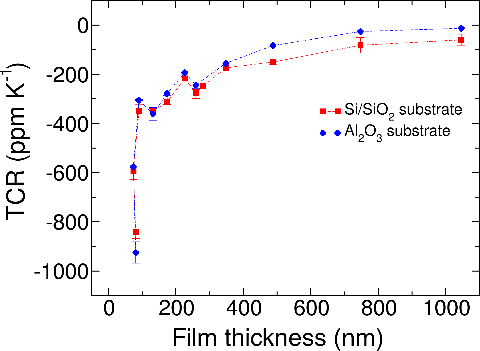
Figure 4Temperature coefficient of resistivity (TCR) of Ni:a–C:H films with 55 ± 5 at. % Ni versus film thickness for different types of substrates.
The TCRs were evaluated as well and plotted in Fig. 4. For moderate thicknesses, a small negative TCR is observed that can be influenced by the composition. For film thicknesses less than 100 nm, a sharp decrease to higher negative values is obvious. This decline may be attributed to the beginning of an island-like growth of a film (Witt, 1974). Yet we suppose an additional reason. If the films are so very thin, the initial layer is presumably not representative for the whole film. At the start of film growth, we consider more carbon-rich phases or even carbon-only phases, as substantiated by our TEM analysis of the interface of substrate and film. In the initial phase of the deposition, carbon would be deposited onto the hot surfaces, prior to the forming of Ni-clusters. As carbon has a negative TCR, this behavior would dominate in very thin film regimes.
As already shown (Koppert et al., 2012), the TCR is nearly constant over a wide range of temperatures from 100 to approx. 450 K, a very important feature for temperature compensated strain gauges and sensors. It is further possible to adjust the TCR of the films by means of the metal to carbon ratio. The influence on the resistance due to thermal expansion coefficients of different substrate materials like steel, aluminum, and others may thus be compensated. In this way, it is possible to get an apparent strain near zero in an appropriate temperature range.
3.3 Longitudinal and transversal gauge factors
The same setup was employed to study the anisotropy of the strain sensitivity of Ni:a–C:H thin films (approx. 150 nm thick) with a nickel concentration of 55 ± 5 at. % on Si/SiO2 substrates. In order to differentiate the gauge factors, we designed two different measurement structures (inset of Fig. 5), one with a direction of strain and current flow in parallel (1 mm × 5 mm) and another with a perpendicular arrangement (0.5 mm × 4 mm). The gauge factor in the longitudinal case kL reveals values of 27.5 ± 2, while in the transverse direction kT is 13 ± 1 thus about 50 % of the longitudinal factor. This result indicates an important sensitivity contribution of granular Ni:a–C:H films when the current flows perpendicular to the strain direction. Although metal foils of conventional strain gauges such as constantan or CrNi have a negligible transverse strain sensitivity (with a ratio kT∕kL < 0.002; HBM, 2016), a comparably large transverse factor is characteristic for Ni:a–C:H thin films.
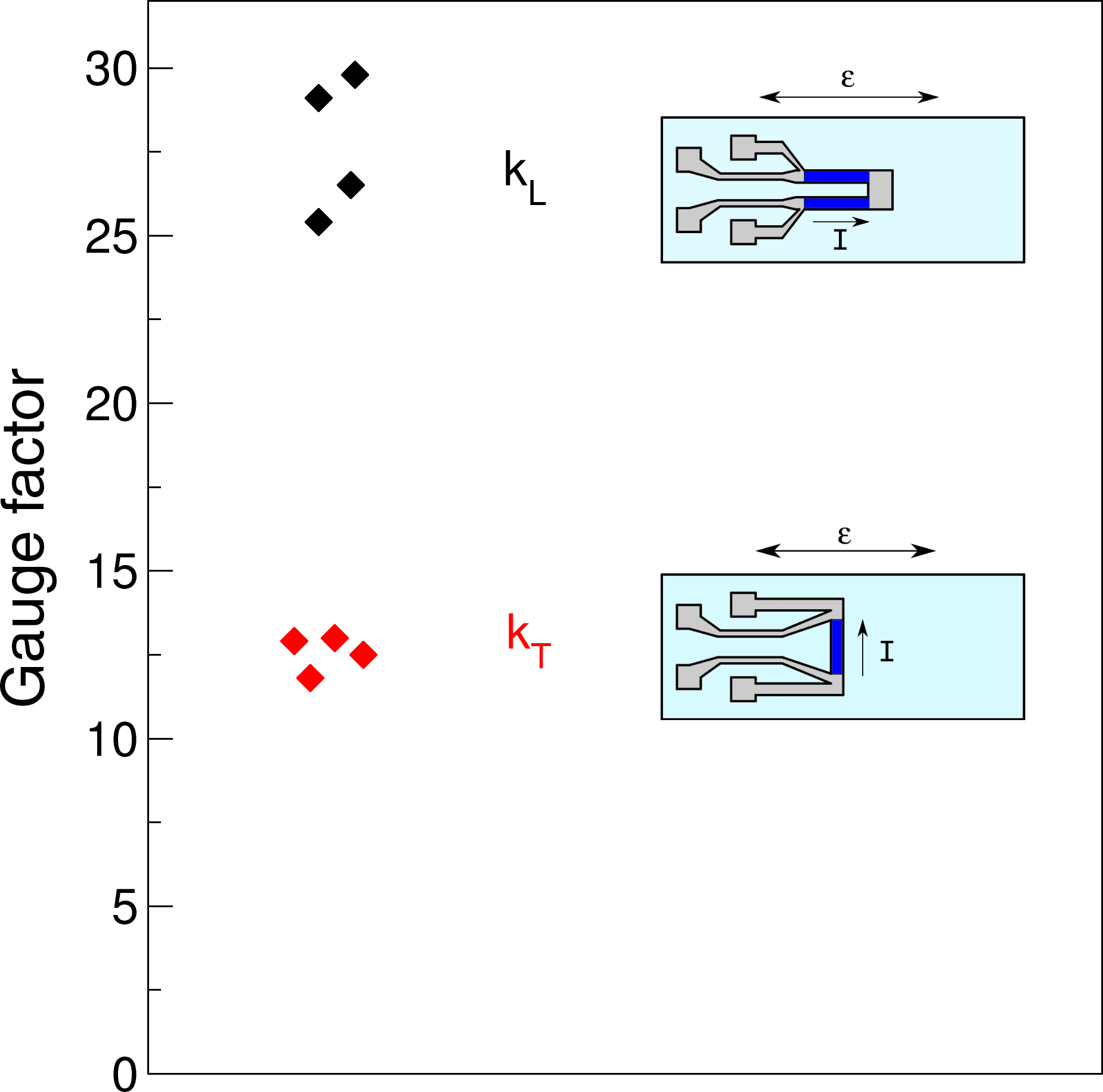
Figure 5Longitudinal gauge factors kL and transverse kT of Ni:a–C:H films (with 55 ± 5 at. % Ni). The respective measurement structures are depicted.
The reason for such an important resistance change of granular films if strain is applied perpendicular to the current direction provides an insight into the conduction mechanism. The conduction depends on particle-to-particle paths that are not in straight lines but follow various detours (Jiang et al., 2015; Grimaldi et al., 2001; Grimaldi, 2014) due to the random arrangement of particles. If strain is applied transverse to the current direction, the transverse detour-components of the conduction paths are strained as well, resulting in a resistance change with a transverse gauge factor kT. For a further analysis and modeling, we refer to our associated paper by Schwebke et al. (2018).
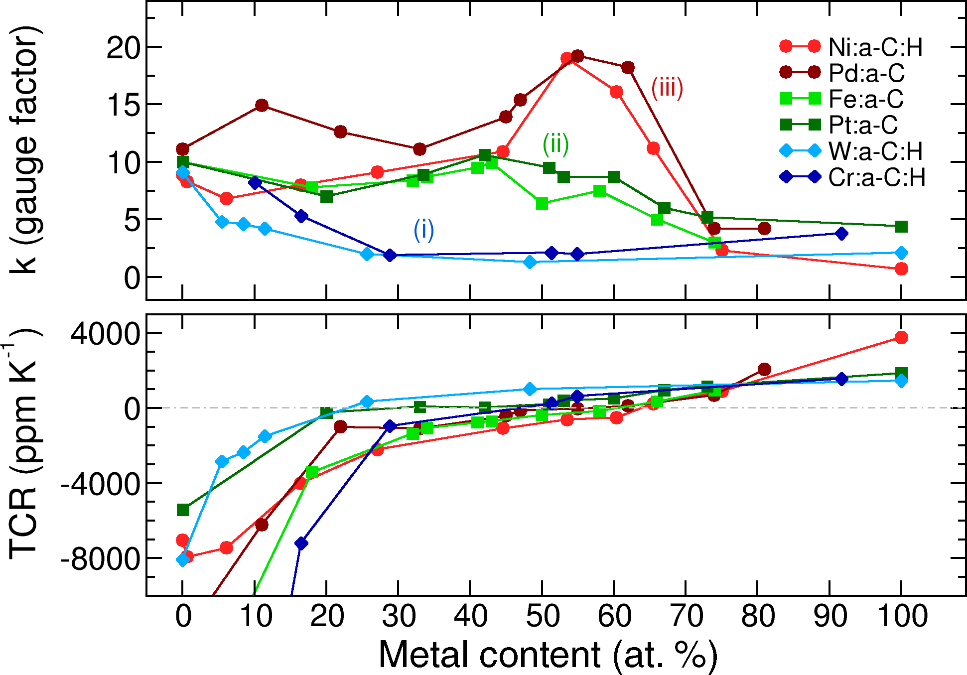
Figure 6Gauge factors and TCRs of six different metal–carbon systems versus metal concentration. The grouping (i)–(iii) is according to the text. Hydrogen incorporation due to a reactive process is indicated by H in the legend of different films. Only Ni and Pd show a sensitivity peak at 55 ± 5 at. % of metal together with a zero crossing of the TCR. The samples were prepared on substrates of Al2O3 with a roughness Ra of 75 nm. If these films are prepared on very smooth substrates, the gauge factors would increase to approx. 30, as depicted in Fig. 3.
3.4 Metal concentration series for different metal–carbon combinations
Many different transition-metal targets were applied successively in the sputtering tools to produce and analyze concentration series with the elements Ni, Pd, Fe, Pt, W, and Cr whereas some other elements Co, Au, Ag, Al, Ti, and Cu were briefly studied. Either the reactive process yielding films of Ni:a–C:H (with a hydrogen concentration of about 12 at. %; Koppert et al., 2012), W:a–C:H, and Cr:a–C:H or the co-sputtering process without hydrogen incorporation was applied as described above. For each material, we prepared a series of about 10 samples with varying metal to carbon concentrations. We measured the response of unidirectional strain on resistors in the form of the U-shape as well as the TCRs. All depositions with film thicknesses from 150 to 300 nm were performed on alumina substrates.
The panels of Fig. 6 reveal some common features. The gauge factor starts at about 10 ± 2 for metal free a–C:H and a–C films; hence, this value is assigned to the carbon matrix associated with a highly negative TCR. At the metal-rich side of the panels, we observe low gauge factors for all metals due to percolated phases connected with positive TCRs as is characteristic for metal layers. Besides these common features, we perceive three differently behaving metal–carbon groups. (i) In the case of Cr:a–C:H and W:a–C:H, only very low gauge factors are measured, except for the carbon-dominated side of the panel. Owing to the high affinity between these transition metals and carbon, W and Cr are known to form stable and well conducting carbides (Andersson et al., 2012; Magnuson et al., 2012) of WC and Cr3C2, respectively. The incorporation of such metals into carbon would probably ameliorate the electrical stability but they are not able to enhance the strain sensitivity. (ii) Fe–C and Pt–C represent another group. These metal–carbon combinations have constant gauge factors around 10 up to the percolation limit at about 70 at. %, comparable to Schwalb et al. (2010). The gauge factor of the carbon matrix is essentially maintained until gradually more and more conduction paths percolate. Iron is known to form the stable carbide cementite Fe3C, but under specific conditions (Mattevi et al., 2011) graphitic carbon may precipitate from Fe. In the case of the precious metal platinum, we expect to have Pt nanoparticles in the carbon matrix. We will substantiate these assumptions later on with our morphology investigations. (iii) A substantial enhancement of sensitivity at 55 ± 5 at. % is revealed for the third group consisting of Ni:a–C:H and Pd:a–C. Hence, this group comprises the most preferable metal components in terms of gauge factor and TCR as depicted in Fig. 6. As already laid out in our previous work (Koppert et al., 2012), Ni–C consists of two phases: a crystalline nanoparticle phase of either fcc–Ni or Ni3C (depending on the deposition conditions) and an embedding carbon phase. Interestingly, the Ni–C deposition was also performed in the co-sputter tool (with DC-power), yielding Ni:a–C (without hydrogen) with about the same values for the gauge factor of 20 at around 60 at. % of Ni. Yet in another variation, we employed a reactive RF-process (with magnetron in this case) and reproduced the same values for the gauge factors. The results with nickel are hence irrespective of whether the film contains hydrogen, or what kind of plasma process is chosen. The palladium samples exist as crystalline fcc–Pd nanoparticles in the carbon matrix as shown by electron diffraction in our TEM analysis.
For the sake of clarity, we do not present the results of the other probed elements in the same figure; instead, we report as follows: the results with Co–C are very similar to Fe–C. The composites of Au–C and Ag–C possess very unstable electrical resistances, probably due to high diffusion rates of these atoms in carbon. Hence, they are not applicable for our purpose of stable strain gauges. With Al–C, Ti–C, and Cu–C we got significant changes of resistances and TCRs at moderate heating temperatures. These elements are obviously prone to oxidation in the carbon matrix and thus not preferred either.
Gauge factors of 20 are thus the highest values in our element and concentration study (on rough alumina substrates with U-shaped structure) and these values are specific to Ni- and Pd–carbon systems. These gauge factors are enhanced to about 30 if deposited onto substrates with smooth surfaces as shown in Fig. 3. The metals Ni and Pd are obviously outstanding and the question arises, what is particular with these elements regarding the interaction with carbon? Transition elements have different solubility in carbon and different affinity to carbon reflected by the fact that they form either stable, metastable carbides, or no carbide phases at all (Mattevi et al., 2011). In addition, the ability to expel or precipitate carbon to form sp2-bonded crystalline carbon, i.e., graphene or graphite from a solid solution, depends on their carbon affinity. The catalytic power of transition metals for the formation of crystalline graphite at the interfaces is thus quite distinct. The affinity towards carbon decreases in the sequence Cr, Fe, Co, Ni, and Cu, whereof Cu has the lowest affinity to carbon and does not form any carbide phases at all. Fe, Co, and Ni form metastable carbides. Following Mattevi et al., the most suitable catalyst for graphite formation are those metals (Ni, Cu) that have low affinity towards carbon but are still able to stabilize carbon on their surfaces by forming weak bonds. The three distinct groups of Fig. 6 thus seem to represent elements with different affinities towards carbon and their corresponding capability to catalyze GLC at their interfaces. In order to gain a deeper knowledge of the film structures, the morphology of some of the metal–carbon films was studied by means of TEM and XRD.
3.5 Film morphology
TEM provides in-depth knowledge of the film morphology. We start with the analysis of our group (iii) metals. A Ni:a–C:H film with 55 ± 5 at. % of nickel prepared as a 70 nm thin film on a TEM membrane of Si3N4 and a pre-heating of 400 ∘C is chosen as an example. The gauge factor of a sample prepared together with the TEM specimen but on alumina is 16. In the top-view representation of Fig. 7a, circular structures of nickel carbide (Ni3C) nanoparticles appear dark and light-colored carbon walls separate them. High-resolution TEM (Fig. 7b) reveals the metal-containing clusters are embedded in graphitic carbon ordered like shells around the clusters. The nanoparticles are thus encapsulated all around by several monolayers of GLC. The mean diameter of the clusters is about 15 nm, but individual clusters range between 5 and 23 nm in this sample. The examination of specimens from different depositions yielded mean diameters of 11 to 22 nm. Amorphous carbon domains exist at the junctions of the carbon shells. The nearest distance between clusters – which is the most important distance for the conduction processes – is estimated between 1 and 2 nm. This corresponds to a number of 3 to 6 lattice planes of crystalline graphite with distances between 0.35 and 0.39 nm. The lattice constants are higher than the literature value of graphite (0.335 nm; Delhaes, 2000), possibly due to adsorbed hydrogen atoms that increase the lattice plane separation (Aga et al., 2007), bending of layers, and other defects. Figure 7c represents a TEM electron diffraction of a (heat treated) Ni–C specimen. The inner diffuse ring corresponds to the lattice spacing of 0.35 nm of graphite. All other diffraction rings are associated with crystalline, either Ni3C or fcc–Ni, nanoparticles. Both phases can develop during deposition; however, fcc–Ni is the thermodynamically stable phase emerging at processes with higher substrate temperature.
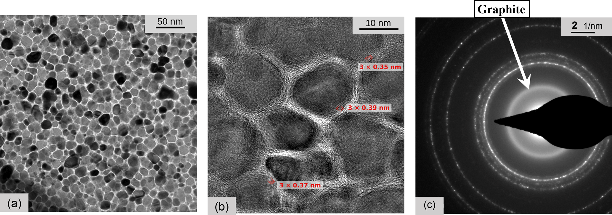
Figure 7TEM micrographs of Ni:a–C:H films in top view. The gauge factor of a sample prepared simultaneously on an Al2O3 substrate is 16. (a) Nearly circular clusters are separated by carbon walls. (b) The high-resolution image reveals that carbon lattice planes are arranged around the particles whereas amorphous carbon regions are found at the junctions of carbon interlayers with different orientation. (c) TEM electron diffraction of Ni:a–C:H. The inner ring represents crystalline graphite with a lattice spacing of 0.35 nm. All other diffraction pattern are matching different crystal lattice planes of either fcc–Ni or Ni3C.
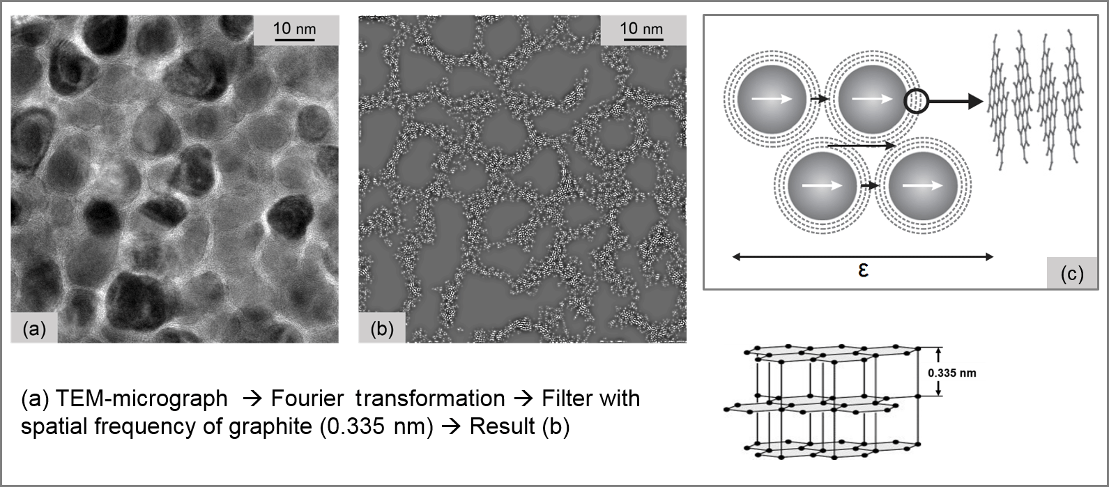
Figure 8(a) High-resolution TEM micrograph of Ni:a–C:H film in top view. (b) Result of the image processing by Fourier transformation with subsequent filtering with the spatial frequency of graphite (0.355 nm). The white dots represent the characteristic distance of the basal planes. (c) Model of the film morphology and conduction paths.
In order to assure our finding of the complete GLC encapsulation, the data of a top-view TEM (Fig. 8a) were Fourier transformed and filtered with the spatial frequency of graphite (spacing around 0.335 nm). The result is presented in Fig. 8b, with the same scale as Fig. 8a. White dots in this picture represent lattice separations with just the filtered distance, i.e., the separation of basal planes of graphite. Therefore, we establish the model of Fig. 8c; nanocrystals are surrounded all over with some layers of GLC. The electron transport in such a material is complicated. Besides well conducting paths within the particles and along the graphitic basal planes there are barriers across the planes, which the electrons have to tunnel (see Fig. 8c). We think these tunnel processes are the reason for the increased strain sensitivity, because the separation of graphitic layers would increase if strain is applied.
From the top view, it is unclear whether the film is built of spheres or columns perpendicular to the plane. Therefore, cross-section samples were prepared by means of a focused ion beam system, after coating with a protective platinum film. The cross section (Fig. 9) shows a 280 nm Ni:a–C:H film on alumina (C2H4/Ar: 3.875 %; pre-heating: 300 ∘C, 60 min; post-heating: 300 ∘C, 30 min). The corresponding longitudinal gauge factor is 15. The micrograph reveals three distinguishable sub-layers: a 240 nm columnar layer near the substrate surface and a 40 nm layer at the top of the film with a globular structure. Carbon shells surround both the polycrystalline columnar and the globular structures. The columnar nickel particles are oriented vertical to the local substrate surface and are separated from each other by the GLC phase. A third very thin sub-layer (∼ 20 nm) may be perceptible at the substrate interface. This layer consists of more or less spherical particles because the carbon concentration is presumably higher at the very beginning of the deposition. This seed sub-layer is likely the reason for the strongly negative TCR of very thin films of Fig. 4.
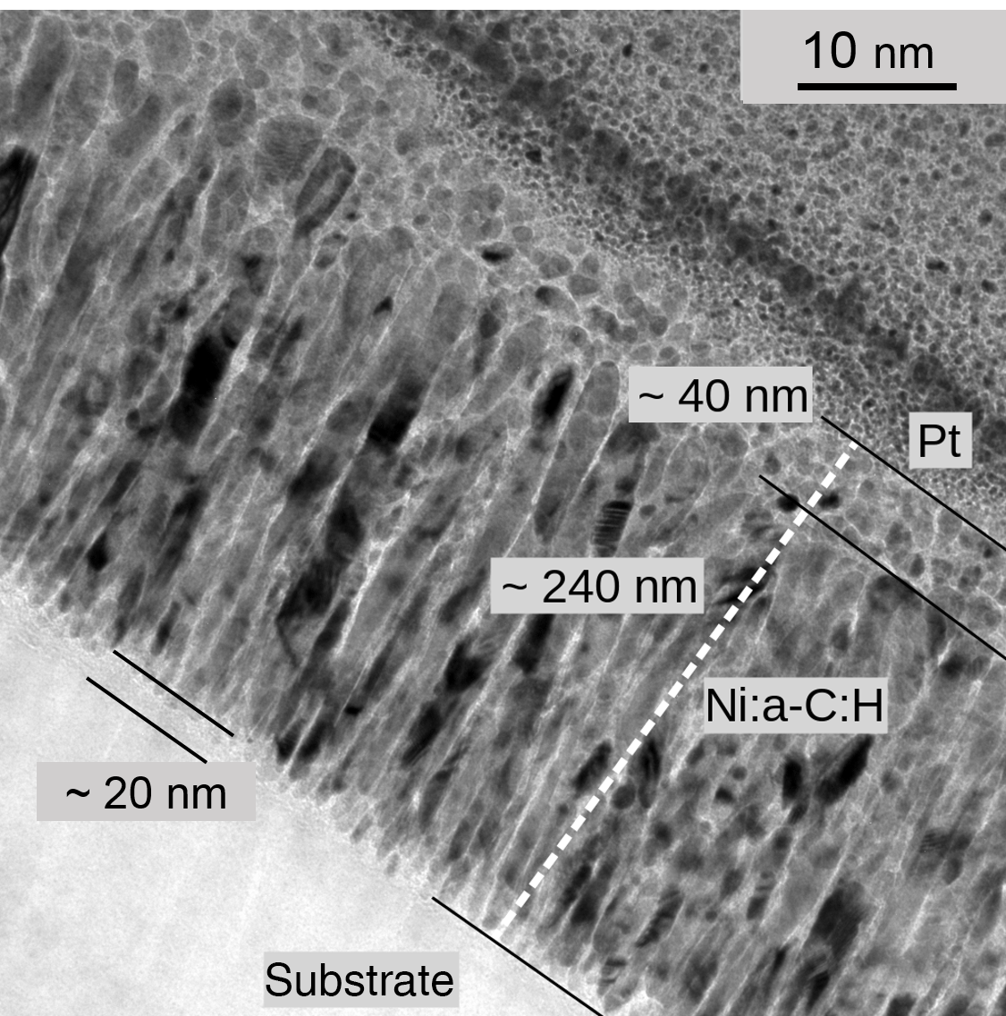
Figure 9Vertical cross-section TEM micrograph of Ni:a–C:H (with 55 ± 5 at. % Ni). Three sub-layers are indicated according to the text.
According to El Mel et al. (2012), the geometry of the metal particles in a nickel–carbon film strongly depends on the carbon content. For films deposited at room temperature, the authors observed spherical clusters for metal contents below 46 %, whereas columnar structures are favored above 65 %. However, in our heated processes with temperatures of about 250 ∘C, the nanoparticles will elongate in the growth direction forming an array of nanocolumns (Abrasonis et al., 2009), even with lower metal content than 65 %. The very different thicknesses of our two sub-layers of the ratio 6 : 1 for the columnar and spherical layer is understood as follows. The surface of the nickel target might get enriched progressively with carbon during the sputtering process. Hence, a gradual decrease in the proportion of nickel to carbon would occur, inducing the formation of spherical structures below a certain metal concentration. Still a different explanation might be plausible as well. During the whole deposition process, more or less spherical nanoparticles might temporarily form on top of the growing film. Then, as the process goes on, these particles might coalesce and build the contiguous columns, except for the very last top layer.
Our TEM analysis was continued with samples of Pd:a–C, again on Si3N4 membranes deposited at a temperature of 250 ∘C. The palladium nanoparticles are smaller compared to nickel, but the striking difference is in the separation layers (Fig. 10a). It is hard to find intact graphitic lattice planes. Instead, we only see few fragments or debris of lattice planes with the characteristic distance of about 0.36 nm. Fourier processing and filtering as explained above yielded no result either. Still another point is noticeably different: from two out of three test objects, sub-layers readily split apart and decompose further into small pieces. We think that this fragmentation occurs not accidentally but is probably due to high mechanical stresses in the samples. This may be the reason for the degeneration and instability of Pd:a–C films starting at temperatures of about 140 ∘C in ambient air. The complete electron diffraction pattern in Fig. 10b is associated with the lattice constants of crystalline fcc–Pd. No diffraction evidence is found for crystalline graphitic carbon.
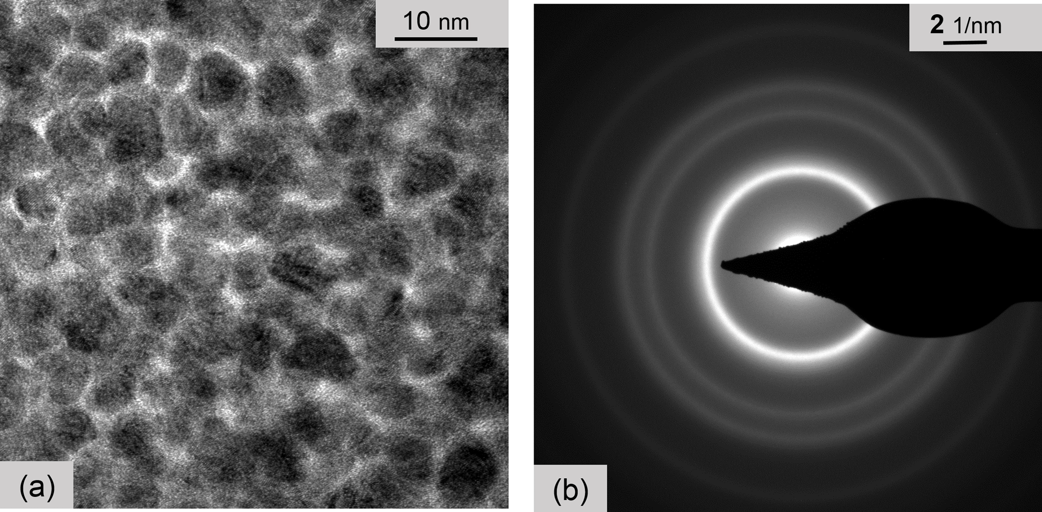
Figure 10(a) TEM micrograph of a Pd:a–C film in top view. (b) TEM electron diffraction of Pd:a–C. All diffraction rings are associated with crystalline fcc–Pd nanoparticles. No evidence of graphitic carbon is found.
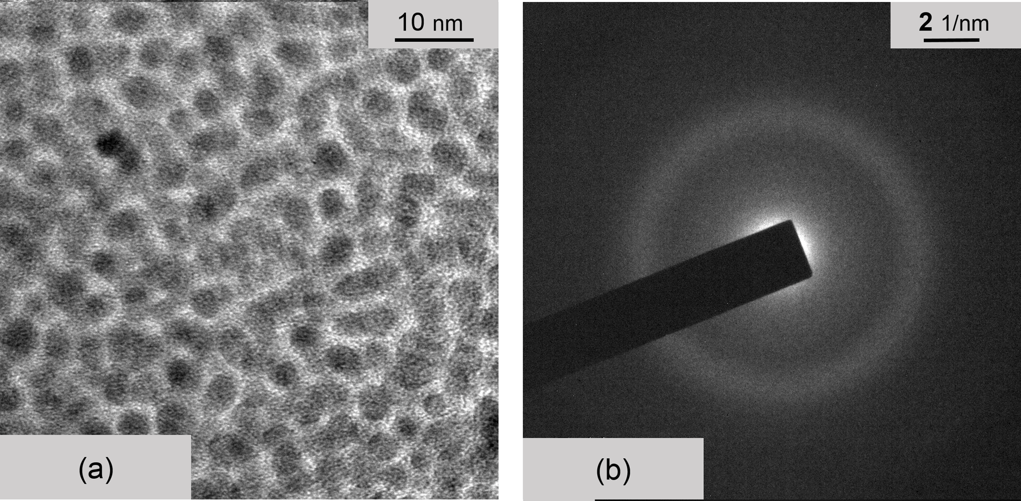
Figure 11(a) TEM micrograph of a Cr:a–C:H film in top view. (b) TEM electron diffraction of Cr:a–C:H. The sample is dominantly amorphous. The weak diffuse ring may be associated with either Cr or Cr3C2.
XRD scans of the group (ii) compound Fe:a–C:H reveal different iron carbides of the nanoparticles. The TEM micrographs have a significantly lower contrast compared to the Ni–C specimens. There are only very few indications for a thin graphitic separation layer with the characteristic lattice constant of graphite, therefore the nanoparticles are again not encapsulated by intact graphitic-like separation layers. The carbon phase is dominantly amorphous. XRD of Pt:a–C reveals very clearly the existence of fcc–Pt nanoparticles within an amorphous carbon matrix. The dimensions of the Pt-nanoparticles are estimated to be 11.4 nm (for 51 at. % Pt). For both materials of our group (ii), we thus have metal–carbide or metal particles in amorphous carbon without any hint of a specific interface as in the case of Ni–C.
Finally, the carbon affine elements (i) are presented. The TEM micrograph of Cr:a–C:H (Fig. 11) looks comparable to Fe:a–C:H. The sample is predominantly amorphous and is to describe as an almost amorphous Cr–C phase of nanoparticles (presumably Cr3C2) within an amorphous carbon (a–C) phase. The electron diffraction pattern of Fig. 11b shows only one very weak and diffuse diffraction ring associated with Cr.
Chromium is one of the transition metals with high affinity to carbon and thus forms a chemically very stable carbide, which was described as mainly or completely amorphous by Andersson et al. (2012) and Magnuson et al. (2012). They deposited chromium and carbon by a non-reactive DC-magnetron sputter process. Gudaitis et al. (2012) produced chromium carbide layers by means of an RF-reactive diode sputtering (as we did) and obtained gauge factors ranging from 2 for chromium rich layers up to 8 for carbon rich layers. Thus, our results on chromium carbide fit into the work of the cited authors. For the other probed strong carbide former W, we also got dominantly amorphous phases. XRD runs of W:a–C:H only show broad peaks associated with WC in an amorphous carbon phase. We summarize the morphology results in Table 1.
We differentiate three groups of metals due to their differing interaction with carbon. The first group (i) includes metals with a strong affinity to carbon. The material consists of two phases: a carbon matrix and carbide nanoparticles, both of them amorphous. Their gauge factors are nearly metallic-like. The group (ii) consists of metals like Pt and Fe, which either form crystalline metal- or carbide nanoparticles in an amorphous carbon phase. However, these elements are not able to catalyze amorphous carbon into GLC at their interfaces. Only the elements of group (iii), Ni and Pd, have the capability to form a closed encapsulation of some monolayers of GLC. Apparently, this special sheathing is accountable for gauge factors of up to 30. We assume the elements Ni (and Pd) are best to catalyze amorphous carbon into GLC, a process occurring at the cluster–carbon interface. If this specific structure of core and shell (i.e., clusters and encapsulating GLC) is destroyed, for instance by annealing at high temperatures, the sensing properties are destroyed as well (Koppert et al., 2012). Although the degeneration of Ni–C starts at annealing temperatures of about 250 ∘C, Pd–C already starts to degenerate at 140 ∘C if annealed in ambient air. Thus the best combination, as far as we know, is Ni–C.
The GLC encapsulation provides an anisotropic electrical contact to neighboring nanocrystals. The conductivity of bulk graphite parallel to the planes is high (3 × 10³ Ω−1 cm−1), whereas in the vertical it is 3 orders of magnitude lower (3 Ω−1 cm−1) (Pierson, 1993). Therefore, the GLC barriers hinder the electrical transport. Tunneling and hopping are thus the phenomena that have to be encountered. The carriers have to tunnel, at least in some parts, vertically through the graphitic structure, unless they are not completely bound to the carbon matrix. That tunneling contribution makes metals that are able to form GLC separations much more sensitive to strain. These special barriers are thus electrically different from amorphous ones as illustrated in Fig. 12. If the carbon encapsulation is amorphous, the matrix has an isotropic conductance that is possibly further enhanced due to metallic impurities. In this case, the conduction is dominantly supported by the matrix alone, without the need for tunneling. Thus, no significant enhancement of strain sensitivity should occur.

Figure 12(a) Schematic representation of nanoparticles such as nickel surrounded by GLC as separation layers. Due to a very low conductivity vertical to the basal planes, the carriers have to tunnel from cluster to cluster. Thus, a significant enhancement of the strain sensitivity is observed if the metal concentration is appropriate for group (iii) elements. (b) This scheme provides a representation of clusters embedded in amorphous carbon. Due to the isotropic and higher conductivity of the matrix, carriers do not have to tunnel. The schematic diagram reflects the consequence of the strain sensitivity; in this case, there is no enhancement due to tunneling as is measured for the metal–carbon compositions of group (i) and (ii).
In this research, advanced functional films for strain sensor applications were prepared and examined. The films are considered granular metals with a carbon-based matrix: they consist of nanocomposites of carbon with different metal or metal carbide clusters. Some of these metal–carbon films are able to sense mechanical strain very effectively. The films are piezoresistive; hence, strain acting on the films influences their electrical resistance. The best results in terms of strain sensitivity were achieved with nickel–carbon films (Ni:a–C:H). Gauge factors of up to 30 are demonstrated. The resistance of a gauge is therefore changed by 30 ‰ due to mechanical strain of 1 ‰. Compared to metal alloys of CrNi, the standard functional film for pressure and force sensors, the new nanocomposite is by a factor of 15 more sensitive and therefore very desirable for numerous applications. These nanocomposites have a nearly linear dependence of resistance versus strain, quite different from the exponential dependence of some known colloidal gold nanoparticle films and nano-cermets. Another result comprises a substantial transverse sensitivity in the range of 50 % comparable to other granular systems (Jiang et al., 2015).
We prepared many different transition metal–carbon composites. With Ni, Pd, Fe, Pt, Cr, and W whole concentration series were examined in detail. Other elements like Co, Au, Ag, Al, Ti, and Cu were studied more briefly, because their performance for sensor layers is inadequate. An in-depth analysis of the microscopic structure was performed and vertical cross-section TEM analysis revealed a columnar structure. We have worked out the conditions of elevated strain sensitivity in metal–carbon thin films and discovered the extraordinary role of nickel–carbon. The reason is attributed to the capability of nickel to graphitize carbon and stabilize an encapsulation of GLC around each nickel nanoparticle. Due to the high resistivity perpendicular to graphite planes, tunneling processes contribute to the conduction. Straining the film will thus influence the resistance strongly. With most other metals, the carbon matrix is dominantly amorphous and thus has a lower resistivity and carries the major part of the current. With these metals, the strain sensitivity is at most that of the carbon matrix.
In an associated paper, we are going to model the longitudinal and transverse strain sensitivity in light of the above-presented insights. For the modeling, the matrix material will be considered a weak electrical conductor with a relatively low conductance. This allows a focus on the strain sensitivity due to electron tunneling between metal particles if GLC separation walls exist.
The research data were collected in laboratory books over quite a long period of time. The data are stored in written form and are not available on the internet.
HS-E designed and conducted the experiments with the help of the persons mentioned in the acknowledgments. UW performed the TEM analysis and interpreted the micrographs. SS helped with the analysis and prepared most of the figures. GS prepared the manuscript with contributions from all co-authors. All authors contributed to the discussions.
The authors declare that they have no conflict of interest.
The authors thank Anne-Catherine Probst, Dirk Göttel, Mario Cerino,
Dennis Vollberg, Angela Lellig, and Olivia Freitag-Weber for additional
sample preparation, help with the measurements, XRD, and EDX analysis as
well as for discussions. We thank Thomas Pelt for the contribution of the
tensile experiment on polyimide foil (Fig. 2). We gratefully acknowledge the
help of Marcus Koch (Leibniz Institute INM, Saarbrücken, Germany) for
the TEM analysis of Cr–C (Fig. 11). We thank Shlomo Berger (Technion, Haifa,
Israel) for some additional cross-section TEM analysis. Part of the work was
funded by the Federal Ministry of Education and Research of Germany (BMBF)
under the program VIP (project funding reference number VIP 03V0436) and the
Deutsche Forschungsgemeinschaft (DFG SCHU 1609/4-2). The financial support
is gratefully acknowledged.
Edited by: Ryutaro Maeda
Reviewed by: two anonymous referees
Abrasonis, G., Kovács, G. J., Ryves, L., Krause, M., Mücklich, A., Munnik, F., Oates, T. W. H., Bilek, M. M. M., and Möller, W.: Phase separation in carbon-nickel films during hyperthermal ion deposition, J. Appl. Phys., 105, 083518, https://doi.org/10.1063/1.3110187, 2009.
Aga, R. S., Fu, C. L., Krcmar, M., and Morris, J. R.: Theoretical investigation of the effect of graphite interlayerspacing on hydrogen absorption, Phys. Rev. B, 76, 165404, https://doi.org/10.1103/PhysRevB.76.165404, 2007.
Andersson, M., Högström, J., Urbonaite, S., Furlan, A., Nyholm, L., and Jansson, U.: Deposition and characterization of magnetron sputtered amorphous Cr–C films, Vacuum, 86, 1408–1416, https://doi.org/10.1016/j.vacuum.2012.01.021, 2012.
Bayer, B., Bosworth, D., Michaelis, F., Blume, R., Habler, G., Abart, R., Weatherup, R., Kidambi, P., Baumberg, J., Knop-Gericke, A., Schloegl, R., Baehtz, C., Barber, Z., Meyer, J., and Hofmann, S.: In Situ Observations of Phase Transitions in Metastable Nickel (Carbide)/Carbon Nanocomposites, J. Phys. Chem. C, 120, 22571–22584, https://doi.org/10.1021/acs.jpcc.6b01555, 2016.
Delhaes, P.: Graphite and Precursors, CRC Press, Amsterdam, the Netherlands, 2000.
Dimigen, H., Hübsch, H., and Memming, R.: Tribological and electrical properties of metal-containing hydrogenated carbon films, Appl. Phys. Lett., 50, 1056, https://doi.org/10.1063/1.97968, 1987.
El Mel, A. A., Bouts, N., Grigore, E., Gautron, E., Granier, A., Angleraud, B., and Tessier, P. Y.: Shape control of nickel nanostructures incorporated in amorphous carbon films: From globular nanoparticles toward aligned nanowires, J. Appl. Phys., 111, 114309, https://doi.org/10.1063/1.4728164, 2012.
Garlow, J. A., Barrett, L. K., Wu, L., Kisslinger, K., Zhu, Y., and Pulecio, J. F.: Large-Area Growth of Turbostratic Graphene on Ni(111) via Physical Vapor Deposition, Sci. Rep., 6, 19804, https://doi.org/10.1038/srep19804, 2016.
Grimaldi, C.: Theory of percolation and tunneling regimes in nanogranular metal films, Phys. Rev. B, 89, 214201, https://doi.org/10.1103/PhysRevB.89.214201, 2014.
Grimaldi, C., Ryser, P., and Strässler, S.: Gauge factor enhancement driven by heterogeneity in thick-film resistors, J. Appl. Phys., 90, 322–327, https://doi.org/10.1063/1.1376672, 2001.
Gudaitis, R., Meskinis, S., Slapikas, K., Andrulevicius, M., Niaura, G., and Tamulevicius, S.: Piezoresistive and electrical properties of Cr containing diamond-like carbon films, Surf Coat. Technol., 211, 80–83, https://doi.org/10.1016/j.surfcoat.2011.08.040, 2012.
HBM GmbH: Katalog für Dehnungsmessstreifen und Zubehör, http://www.hbm.com/fileadmin/mediapool/hbmdoc/technical/s1264.pdf (last access: 1 October 2017), 2016.
Heckmann, U., Bandorf, R., Petersen, M., Gwozdz, V., and Brauer, G.: Matching of maximum gauge factor and TCR zero crossing of Me–DLC, in: 2011 IEEE Sensors, Limerick, Ireland, 472–475, https://doi.org/10.1109/ICSENS.2011.6126973, 2011.
Herrmann, J., Müller, K.-H., Reda, T., Baxter, G. R., Raguse, B., d. Groot, G. J. J. B., Chai, R., Roberts, M., and Wieczorek, L.: Nanoparticle films as sensitive strain gauges, Appl. Phys. Lett., 91, 183105, https://doi.org/10.1063/1.2805026, 2007.
Jansson, U. and Lewin, E.: Sputter deposition of transition-metal carbide films – A critical review from a chemical perspective, Thin Solid Films, 536, 1–24, https://doi.org/10.1016/j.tsf.2013.02.019, 2013.
Jiang, C.-W., Ni, I.-C., Tzeng, S.-D., and Kuo, W.: Nearly isotropic piezoresistive response due to charge detour conduction in nanoparticle thin films, Scient. Rep., 5, 11939, https://doi.org/10.1038/srep11939, 2015.
Koppert, R., Goettel, D., Freitag-Weber, O., and Schultes, G.: Nickel containing diamond like carbon thin films, Solid State Sci., 11, 1797–1800, https://doi.org/10.1016/j.solidstatesciences.2009.04.022, 2009.
Koppert, R., Uhlig, S., Schmid-Engel, H., Göttel, D., Probst, A.-C., Schultes, G., and Werner, U.: Structural and physical properties of highly piezoresistive nickel containing hydrogenated carbon thin films, Diamond Relat. Mater., 25, 50–58, https://doi.org/10.1016/j.diamond.2012.01.031, 2012.
Magnuson, M., Andersson, M., Lu, L., Hultman, L., and Jansson, U.: Electronic structure and chemical bonding of amorphous chromium carbide thin films, J. Phys., 24, 225004, https://doi.org/10.1088/0953-8984/24/22/225004, 2012.
Mattevi, C., Kim, H., and Chhowalla, M.: A review of chemical vapour deposition of graphene on copper, J. Mater. Chem., 21, 3324–3334, https://doi.org/10.1039/C0JM02126A, 2011.
Petersen, M., Heckmann, U., Bandorf, R., Gwozdz, V.,Schnabel, S., Bräuer, G., and Klages, C.-P.: Me-DLC films as material for highly sensitive temperature compensated strain gauges, Diamond Relat. Mater., 20, 814–818, https://doi.org/10.1016/j.diamond.2011.03.036, 2011.
Petersen, M., Bandorf, R., Bräuer, G., and Klages, C.-P.: Diamond-like carbon films as piezoresistors in highly sensitive force sensors, Diamond Relat. Mater., 26, 50–54, https://doi.org/10.1016/j.diamond.2012.04.004, 2012.
Pierson, H. O.: Handbook of carbon, graphite, diamond, and fullerenes: properties, processing, and applications, edited by: William, A., Noyes Publications, Albuquerque, New Mexico, p. 61, 1993.
Puyoo, E., Malhaire, C., Thomas, D., Rafaël, R., R'Mili, M., Malchère, A., Roiban, L., Koneti S., Bugnet, M., Sabac, A., and Le Berre, M.: Metallic nanoparticle-based strain sensors elaborated by atomic layer deposition, Appl. Phys. Lett., 110, 123103, https://doi.org/10.1063/1.4978778, 2017.
Schultes, G., Frey, P., Goettel, D., and Freitag-Weber, O.: Strain sensitivity of nickel containing amorphous hydrogenated carbon (Ni:a–C:H) thin films prepared by r.f. sputtering using substrate bias conditions, Diamond Relat. Mater., 15, 80–89, https://doi.org/10.1016/j.diamond.2005.07.005, 2006.
Schwalb, C. H., Grimm, C., Baranowski, M., Sachser, R., Porrati, F., Reith, H., Das, P., Müller, J., Völklein, F., Kaya, A., and Huth, M.: A Tunable Strain Sensor Using Nanogranular Metals, Sensors, 10, 9847–9856, https://doi.org/10.3390/s101109847, 2010.
Schwebke, S., Werner, U., and Schultes, G.: Granular metal–carbon nanocomposites as piezoresistive sensor films – Part 2: Modeling longitudinal and transversal strain sensitivity, J. Sens. Sens. Syst., accepted, 2018.
Witt, G. R.: The electromechanical properties of thin films and the thin film strain gauge, Thin Solid Films, 22, 133–156, https://doi.org/10.1016/0040-6090(74)90001-7, 1974.